
FM PLL controlled VCO

The circuit described is a voltage-controlled oscillator (VCO) that operates within the FM band, specifically between 88 MHz and 108 MHz. This range is typical for FM radio transmissions. The core of the oscillator is a Colpitts configuration, which is known for its stability and ease of tuning. The use of a BC817 transistor, while not ideal for high-frequency applications, demonstrates the circuit's robustness and flexibility in component selection.
The LC tank circuit, which is crucial for determining the oscillation frequency, comprises an inductor (L1) and capacitors (C4, C5) in conjunction with a varicap diode (D1). The varicap diode's capacitance varies with the applied reverse voltage, allowing the frequency of oscillation to be adjusted dynamically. The additional varicap (D2) in the audio modulation unit enables the circuit to modulate the frequency based on audio input, facilitating the transmission of audio signals over the FM band.
The PLL (Phase-Locked Loop) component is essential for maintaining frequency stability and precision. By comparing the VCO output frequency with a stable reference frequency from the VCTCXO, the PLL can adjust the VCO's tuning voltage to lock onto the desired frequency. This feedback mechanism ensures minimal drift and high fidelity in the transmitted signal.
The RF power amplifier stage, utilizing a transistor like Q2, amplifies the modulated signal for transmission. The design considerations, including the choice of emitter resistors, determine the output power levels and efficiency of the amplifier. Overall, this circuit exemplifies the integration of various electronic components to achieve a functional and efficient FM transmission system.The main oscillator is printed in blue and is voltage controlled. In this construction the VCO range is 88 to 108 MHz. As you can see from the blue arrows, some energy goes to an amplifier and some energy goes to the PLL unit. You can also see that the PLL can control the frequency of the VCO. What the PLL do is that it compare the VCO frequency with the reference frequency (which is very stable) and then regulated the VCO voltage to lock the oscillator at desired frequency.
The last part that will affect the VCO is the audio input. The amplitude of the audio will make the VCO change in frequnency FM (Frequency Modulation). I will explain it all in detail under section Hardware and schematic. The main oscillator is based around the transistor Q1. This oscillator is called Colpitts oscillator and it is voltage controlled to achieve FM (frequency modulation) and PLL control. Q1 should be a HF transistor to work well, but in this case I have used a cheap and common BC817 transistor which works great.
The oscillator needs a LC tank to oscillate properly. In this case the LC tank consist of L1 with the varicap D1 and the two capacitor (C4, C5) at the base-emitter of the transistor. The value of C1 will set the VCO range. The large value of C1 the wider will the VCO range be. Since the capacitance of the varicap (D1) is dependent of the voltage over it, the capacitance will change with changed voltage.
When the voltage change, so will the oscillating frequency. In this way you achieve a VCO function. You can use many different varicap diod to get it working. In my case I use a varicap (SMV1251) which has a wide range 3-55pF to secure the VCO range (88 to 108MHz). Inside the dashed blue box you will find the audio modulation unit. This unit also include a second varicap (D2). This varicap is biased with a DC voltage about 3-4 volt DC. This varcap is also included in the LC tank by a capacitor (C2) of 3.3pF. The input audio will passes the capacitor (C15) and be added to the DC voltage. Since the input audio voltage change in amplitude, the total voltage over the varicap (D2) will also change.
As an effect of this the capacitance will change and so will the LC tank frequency. You have a Frequency Modulation of the carrier signal. The modulation depth is set by the input amplitude. The signal should be around 1Vpp. Just connect the audio to negative side of C15. Now you wonder why I don't use the first varicap (D1) to modulate the signal? I could do that if the frequency would be fixed, but in this project the frequency range is 88 to 108MHz. If you look at the varicap curve to the left of the schematic. You can easily see that the relative capacitance change more at lower voltage than it does at higher voltage.
Imagine I use an audio signal with constant amplitude. If I would modulated the (D1) varicap with this amplitude the modulation depth would differ depending on the voltage over the varicap (D1). Remember that the voltage over varicap (D1) is about 0V at 88MHz and +5V at 108MHz. By use two varicap (D1) and (D2) I get the same modulation depth from 88 to 108MHz. Now, look at the right of the LMX2322 circuit and you find the reference frequency oscillator VCTCXO.
This oscillator is based on a very accurate VCTCXO (Voltage Controlled Temperature controlled Crystal Oscillator) at 16.8MHz. Pin 1 is the calibration input. The voltage here should be 2.5 Volt. The performance of the VCTCXO crystal in this construction is so good that you do not need to make any reference tuning.
A small portion of the VCO energy is feed back to the PLL circuit through resistor (R4) and (C16). The PLL will then use the VCO frequency to regulate the tuning voltage. At pin 5 of LMX2322 you will find a PLL filter to form the (Vtune) which is the regulating voltage of the VCO. The PLL try to regulate the (Vtune) so the VCO oscillator frequency is locked to desired frequency. You will also find the TP (test Point) here. The last part we haven't discussed is the RF power amplifier (Q2). Some energy from the VCO is taped by (C6) to the base of the (Q2). Q2 should be a RF transistor to obtain best RF amplification. To use a BC817 here will work, but not good. The emitter resistor (R12 and R16) set the current through this transistor and with R12, R16 = 100 ohm and +9V power supply you will easy have 150mW of output power into 50 ohm load.
You can lower the resistors (R12, R16) to get high power, but please don't overload this poor transistor, it will be hot and burn up Current consumption of VCO unit = 60 mA @ 9V. 🔗 External reference
Related Circuits
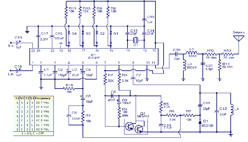
The circuit presented is a high-quality Stereo FM transmitter capable of transmitting signals up to a range of 70 feet. It utilizes the BH1417 PLL stereo transmitter IC from Rohm Semiconductors, which features separate audio processing sections for left...
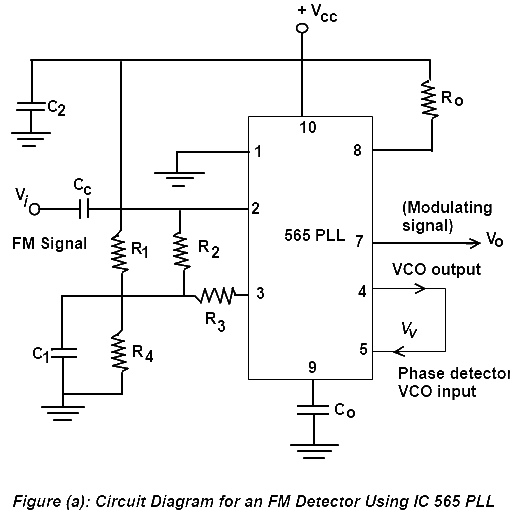
Phase Lock Loop (PLL) FM Detector with 565 PLL IC. The circuit diagram and internal structure of the PLL IC 565 are shown in the given figures. The Phase Lock Loop (PLL) FM Detector utilizing the 565 PLL IC is...

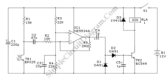
This is a simple automatic light switch circuit designed for bedrooms. After construction, connect the input terminals of this circuit in parallel to the existing light fixture. The automatic light switch circuit operates using a photoresistor (LDR) and a transistor...
This relay circuit is controlled by nearly any type of infrared remote controller. The circuit operates under the assumption that most remote controllers utilize high-frequency signals. The relay circuit described functions by receiving signals from an infrared (IR) remote control,...
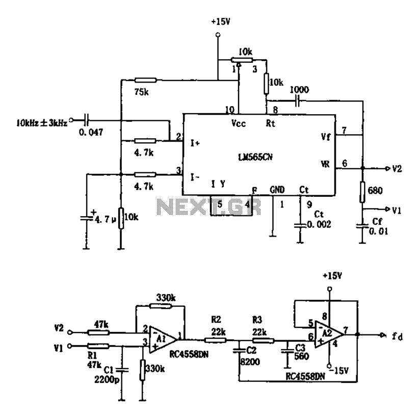
The circuit utilizes a 10 kHz and 3 kHz LM565CN to create an FM demodulation setup. The output diagram (b) illustrates the differential demodulation outputs V1 and V2 from the differential amplifier A1, which provides level displacement and amplification....
The SC9270C/SC9270D is a comprehensive DTMF receiver that integrates both bandsplit filtering and digital decoding functions. The filter section utilizes switched capacitor techniques to achieve high- and low-group filtering along with dial-tone rejection. The decoder employs digital counting techniques...