
FM Transmitter Circuit Type Versatile

The described FM transmitter circuit is a compact and efficient design suitable for various applications. The absence of a coil simplifies the assembly process, making it accessible for hobbyists and professionals alike. The use of gate logic, particularly the CD4069 integrated circuit, allows for a reliable and stable operation. The buffer gate N1 plays a crucial role in amplifying the audio signals captured by the condenser microphone, ensuring that the input signal is adequately strengthened before modulation.
The inverter N2, integral to the circuit, is responsible for generating the radio frequency oscillator within the FM range. This oscillator is essential for creating the carrier wave that will carry the audio information. The BB109 varicap diode is a key component in achieving frequency modulation, as it varies the capacitance in response to the audio signal, effectively modulating the carrier wave frequency to transmit the audio content.
The configuration of inverters N4, N5, and N6 in parallel provides a low output impedance, which is advantageous for driving the antenna efficiently. This configuration minimizes signal loss and enhances the transmission range of the FM signal. The choice of a 10 cm wire as an antenna is practical, as it is sufficient for short-range applications while remaining easy to implement.
Electrolytic capacitors rated at 10V are specified to ensure reliability and performance under typical operating conditions. The recommendation for a 9V transistor radio battery as the power source is due to its ability to provide stable voltage without introducing noise, which is critical for maintaining signal integrity. Overall, this FM transmitter circuit design exemplifies a straightforward approach to building a functional and effective radio transmitter using common electronic components.This is a design circuit diagram of a versatile FM transmitter. This circuit doesn`t have a coil. The circuit is simple and easy to assemble. This circuit is work based on gate logic concept. This is the figure of the circuit. The gate N1 acts as a buffer for strengthening the signals from the condenser microphone. The inverter N2 with its associa ted components forms a radio frequency oscillator in the FM region. The varicaps diode BB109 is used for frequency modulating the audio signal to the carrier wave generated by the oscillator. Inverters N4 t0 N6 are used to drive the antenna. As the N4, N5, N6 are connected in parallel their effective output impedance is very less and can easily drive the antenna.
All electrolytic capacitors must be rated 10V. This circuit is use a 10 cm long wire as antenna. Gates N1 to N6 belong to same IC CD4069. The battery can be a 9V transistor radio battery. Adapters are not recommended because they would induce noise in the circuit. 🔗 External reference
Related Circuits
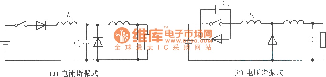
In a commonly used switching stabilized voltage supply, a resonant switch can be utilized to replace the shape of a step-down converter, resulting in a resonant converter circuit. The diagram illustrates the transformation from a step-down converter to a...
The LM3886 high-performance audio power amplifier circuit schematic is a crucial component in sound reproduction within audio systems. This audio power amplifier utilizes the LM3886 integrated circuit to enhance sound quality and output. The LM3886 is a high-performance audio power...
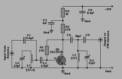
This is a simple circuit of an FM booster designed to enhance the reception of programs from distant FM stations. The amplifier effectively captures signals from far-off FM stations. The configuration is set up as a common-emitter tuned RF...
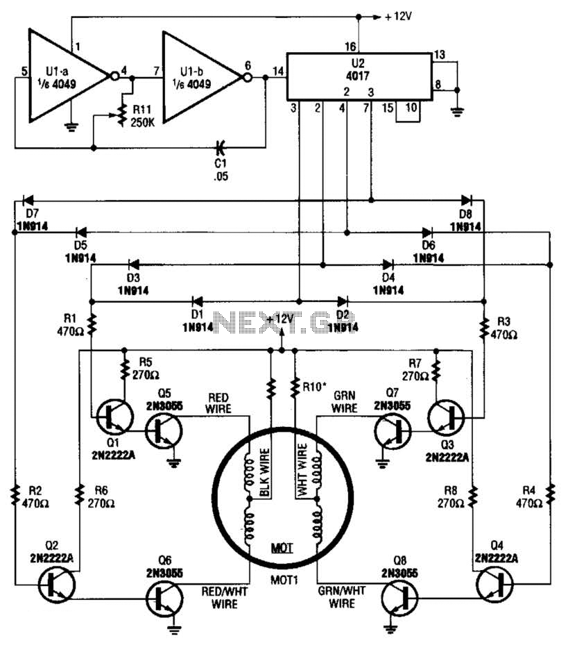
A 4017 decade counter/divider, driven by a low-frequency oscillator (U1-a and U1-b), is employed to control transistor switches that sequence the motor windings as required. The motor (MOT1) is a 12-V stepper motor. Resistors R9 and R10 are chosen...
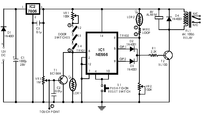
In this circuit, the alarm is activated under four different conditions: 1. When light falls on LDR1 (located at the entry to the premises). 2. When light falling on LDR2 is obstructed. 3. When door switches are opened or...

This circuit diagram of a UPS is designed for use with cordless telephones that cannot operate during a power failure. Since the UPS is intended solely for telephones, its output power is limited to 1.5W. This UPS circuit is...