
UPS Circuit For Cordless Phones PCB
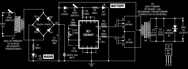
This uninterruptible power supply (UPS) circuit is specifically tailored for cordless telephones, ensuring they remain operational during power outages. The design emphasizes efficiency and cost-effectiveness, making it suitable for assembly on standard printed circuit boards (PCBs). The core of the circuit is the CD4047 integrated circuit, known for its versatility as an astable multivibrator. Operating at a frequency of 50Hz, this IC generates a square wave output that can be utilized to control the power delivery to the telephone.
The configuration of the output stage employs IRF540 MOSFETs, which are arranged in a push-pull configuration. This arrangement allows for effective switching and amplification of the signal generated by the CD4047. The IRF540 MOSFETs are chosen for their high efficiency and ability to handle significant power loads, making them ideal for this application, despite the low output power requirement of only 1.5W.
To protect the circuit from voltage spikes that could potentially damage the components, a metal oxide varistor (MOV) is included in the design. The MOV acts as a transient voltage suppressor, clamping excessive voltages and ensuring that the output remains stable and safe for the connected telephone. This additional filtering stage enhances the reliability of the UPS circuit, providing a clean and stable power supply during interruptions in the mains electricity.
Overall, this UPS circuit design is a practical solution for maintaining the functionality of cordless telephones during power failures, combining efficient power management with robust component selection and protective measures.Circuit This circuit diagram of UPS is designed to use with a cordless telephones that cannot be operated during power failure. Since the ups is only meant for telephone, it`s output power is limiter to 1. 5W. This ups circuit is economical and can be assembled on a general purpose PCB. The circuit works around IC CD4047 which is an astable multivi brator operating at line frequency 50Hz. It`s outputs are capable of driving MOSFETS IRF540 that is configured as push pull type, directly. Here the inverter output is filtered the spikes are reduced using a metal oxide varistor (MOV). 🔗 External reference
Related Circuits
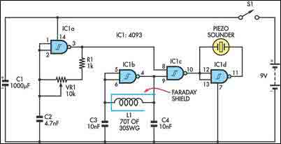
The circuit incorporates two oscillators, both operating at about 40kHz. The first, IC1a, is a standard CMOS oscillator with its frequency adjustable via VR1. The frequency of the second, IC1b, is highly dependent on the inductance of coil L1,...
A CD4016 analog instrument is utilized as a multiplexed digital output, transferring the output function back to the input. The CD4016 operates as a digitally controlled analog transmission gate, eliminating the need for a digital output level shift. Alternatives...
The circuit can also be triggered by logic ICs (TTL/CMOS) using the appropriate interfacing method. Another relay is typically used to serve as the trigger button when interfacing ICs with the latching relay circuit. The described circuit utilizes a latching...
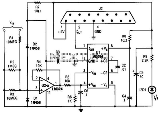
The adapter comprises a voltage-to-frequency converter integrated with a signal conditioning and protection circuit. J2 interfaces with the game port of a personal computer. Additional software references are available for use with this circuit. The voltage-to-frequency adapter functions by converting...
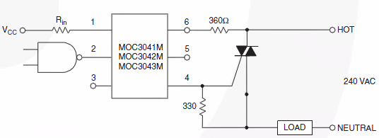
Switch 50V AC voltage. The maximum current drained will be 5A, with a frequency of 50Hz. The switching speed is not critical and can be slow, which is acceptable for the application. Initially, a solid-state relay (SSR) was considered...

This circuit is an active filter designed for subwoofers, featuring a 24 dB per octave Bessel filter with a cutoff frequency of 200 Hz. It is suitable for those interested in experimenting with audio circuits in the subwoofer frequency...
Warning: include(partials/cookie-banner.php): Failed to open stream: Permission denied in /var/www/html/nextgr/view-circuit.php on line 713
Warning: include(): Failed opening 'partials/cookie-banner.php' for inclusion (include_path='.:/usr/share/php') in /var/www/html/nextgr/view-circuit.php on line 713