
FM24C256 interface circuit
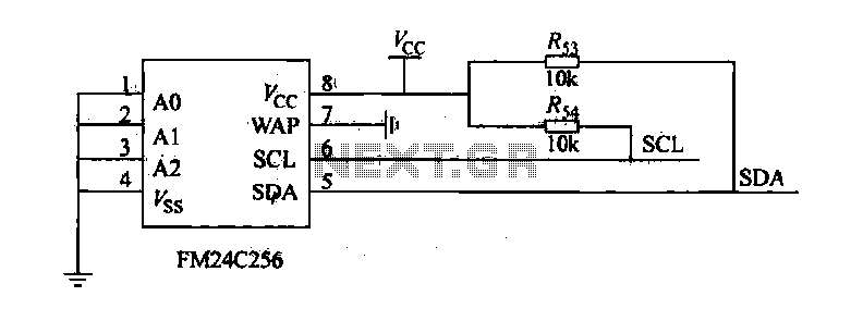
The FM24C256 is a 256 Kbit non-volatile memory device that interfaces with microcontrollers via the I2C communication protocol. In this application, it operates as a slave device, responding to commands from a master device, typically a microcontroller. The configuration of the address pins (A2, A1, A0) determines the device's address on the I2C bus, allowing for multiple devices to coexist on the same bus by assigning them unique addresses.
When the microcontroller initiates communication, it sends a start condition followed by the address byte, which includes the read/write bit. If the read/write bit is set to '1', the FM24C256 prepares to send data to the master device. Conversely, if the bit is '0', the master device is writing data to the FM24C256. The control bit at the lowest address allows the microcontroller to specify the operation type, ensuring that the correct action is taken based on the intended operation.
The MM36SB020 chip complements the FM24C256 by providing storage for Chinese characters in a 16x16 dot matrix format. It is essential for applications that require the display of Chinese characters on screens or other output devices. The control commands for the MM36SB020 are crucial for managing how characters are stored, retrieved, and displayed, allowing for efficient rendering of text in applications where Chinese language support is necessary.
Overall, this configuration illustrates a typical use case of I2C communication for memory management and character display, showcasing the integration of different components to achieve a specific functionality in electronic systems.FM24C256 as shown 27-54 slave interface circuit I2C bus, the address format shown in Table 27-3. A2, Al, AO is set to low (when extended storage capacity, the need to change A2 , A1, AO setting), the lowest address to write control bit, which is. 1 expressed a read operation from the device as a o indicates to be a slave write operation start signal is sent from the controller MCU and after the device address byte. FM24C256 monitors the bus, when its address is sent from the device to match the address when, in response to a signal should blame; perform the appropriate read/write operation according to the state read and write control Pina bit R/Ws.
MM36SB020 chip for storing 16 16 dot matrix Chinese character. Control commands are shown in Table MM36SB020
Related Circuits
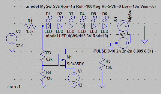
A suitable method to sense when some LEDs in a garage door opener are illuminated. A power source, potentially the same as Vout, connects to a 1.5 kΩ resistor, which then connects to six LEDs followed by a transistor....
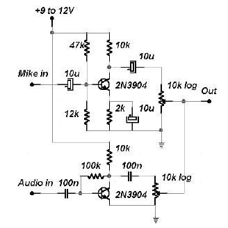
This two-channel audio mixer utilizes 2N3904 transistors to create two preamplifiers. The first preamplifier is designed for high gain, suitable for microphone input, while the second preamplifier allows for control over the audio level input. The audio mixer requires...

An ultra-low-noise, low-distortion operational amplifier, the AD797, is combined with the ADS 11 operational amplifier, which provides high bandwidth and a 100-mA output drive capability. This composite amplifier circuit is effective for driving high-resolution ADCs and ATE systems. The...
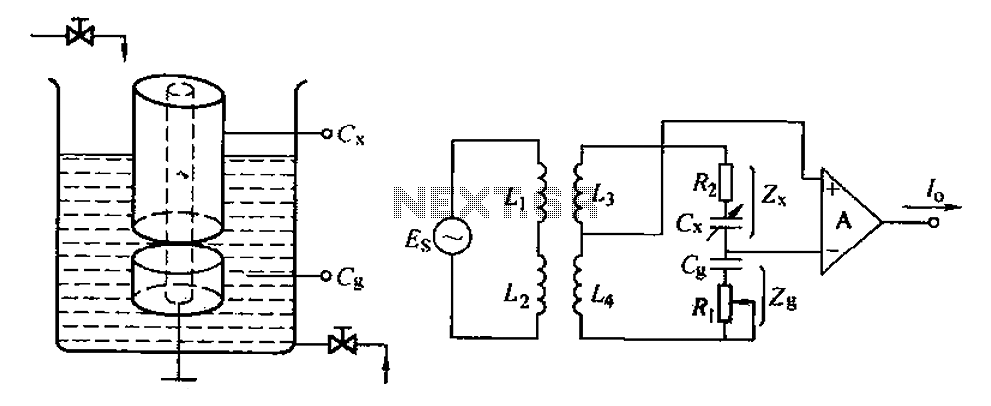
The capacitance change in a capacitive sensor is directly converted into electrical parameters, which are then unified for signal transmission, processing, and display. These electrical parameters can be categorized into resistive, capacitive, and inductive types. This explanation focuses on...
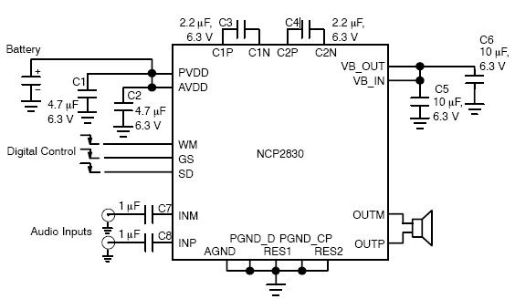
The NCP2830 audio power amplifier features high-quality audio performance with a total harmonic distortion plus noise (THD+N) of 0.04%. It offers low noise with a signal-to-noise ratio (SNR) of up to 100 dB and optimizes overall system efficiency, achieving...
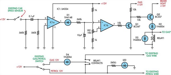
The following circuit illustrates a petrol gas switch sensor circuit diagram designed for a Pajero vehicle. It features a simple configuration utilizing the LM334 integrated circuit and operates automatically. The petrol gas switch sensor circuit is designed to monitor and...
Warning: include(partials/cookie-banner.php): Failed to open stream: Permission denied in /var/www/html/nextgr/view-circuit.php on line 713
Warning: include(): Failed opening 'partials/cookie-banner.php' for inclusion (include_path='.:/usr/share/php') in /var/www/html/nextgr/view-circuit.php on line 713