
FOLDBACK CURRENT LIMITER

The described regulator circuit is designed to provide robust current limiting features, which are essential in protecting both the power supply and the load from excessive current conditions. The operational mechanism is based on the interaction between the components, particularly the resistors and transistors.
Resistor R3 plays a crucial role in sensing the current flowing through the load. As the load current increases, the voltage drop across R3 also increases. Once this voltage reaches a predetermined level, specifically 0.65 V, it activates transistor Q2. The activation of Q2 serves as a feedback mechanism that regulates the output voltage by turning off Q1, which is responsible for supplying power to the load.
This feedback loop is vital for maintaining circuit stability and preventing damage due to overcurrent situations. The foldback characteristics of the circuit allow for a reduction in output voltage as the current draw increases beyond the set limit. This behavior helps to minimize power dissipation in the circuit and enhances the overall efficiency.
It is important to note that the foldback feature not only protects against current surges but also aids in thermal management by reducing the output power delivered to the load under fault conditions. The design of such a regulator circuit is particularly advantageous in applications where the load may experience sudden changes in current demands, ensuring that the system remains within safe operational limits while providing reliable performance.This regulator uses the drop across R3 to sense current draw, turning on Q2, removing drive from Q1, and lowering the output voltage. Limiting occurs when Q2 has 0. 65 V across the base-emitter junction. This circuit has foldback characteristics as seen from the figure. 🔗 External reference
Related Circuits
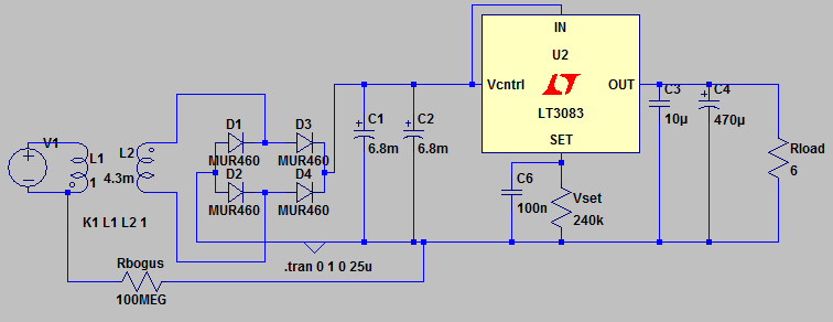
Additionally, it may be necessary to include another input capacitor to mitigate high-frequency noise, although this is not directly related to the main question. The objectives are to achieve a voltage output of 0 - 12 V with a...
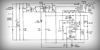
This is a low voltage, high-current output switching DC power supply with an input of 220 volts AC. In this circuit, an ST2 DIAC relaxation oscillator, Q3, C1, and the DIAC initiate conduction of the output switching transistor Q1....
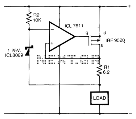
In the circuit presented, a CMOS operational amplifier regulates the current through a p-channel HEXFET power transistor to ensure a constant voltage across the load resistor (RL). The current can be calculated using the formula: I = VREF/RL. The...
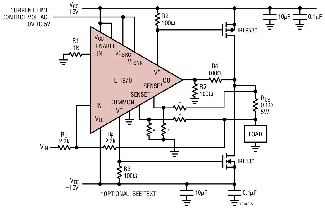
This week, a new favorite chip, the LT1970 power operational amplifier from Linear Technology, is introduced. This device operates from a 36 V supply and can source or sink 500 mA. It features programmable current limiting, outputs for indicating...
Figure 4-52 (a) illustrates the two-phase wiring for direct current (DC) operation, while Figure 4-52 (b) depicts the two-phase current differential wiring for alternating current (AC) operation. The schematic in Figure 4-52 (a) represents a two-phase wiring configuration suitable for...

This is a 1-amp variable-voltage power supply unit (PSU) that can adjust output voltage from approximately 3V to 24V. It features a maximum output current limit, which is particularly useful when powering up a project for the first time...