
four channel oscilloscope
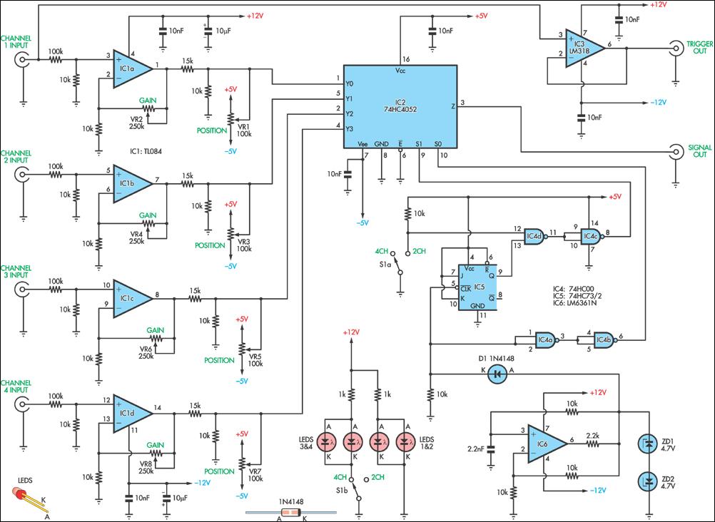
This circuit is designed to facilitate the simultaneous observation of multiple signals, making it particularly useful in applications where low-frequency signals need to be analyzed in a compact manner. The use of the TL084 op-amps ensures low noise and high precision in signal processing. The attenuation and gain adjustment capabilities allow for a wide range of input signal levels, which enhances the circuit's versatility. The integration of an analog multiplexer (IC2) enables efficient channel selection without the need for multiple oscilloscope inputs, thereby streamlining the measurement process.
The oscillator circuit, based on the LM6361, is crucial for generating the timing signals required for channel switching. The frequency of approximately 20kHz is suitable for low-frequency applications, ensuring that the switching does not interfere with the integrity of the signals being observed. The inclusion of zener diodes for voltage clamping protects the logic circuitry from over-voltage conditions, maintaining the integrity of the logic levels used to control the multiplexer.
In conclusion, this circuit provides a robust solution for low-frequency signal measurement, combining effective signal conditioning, precise gain control, and efficient channel multiplexing, making it ideal for various electronic testing and analysis applications.This circuit enables you to display four signals simultaneously using only one channel of your oscilloscope. Essentially, it switches each of the inputs through to the output in turn, with some signal massaging in between.
As shown, it is suitable only for low-frequency signal measurement and does not include over-voltage protection at the inputs. Each input circuit is identical, utilising one amplifier from a TL084 quad op amp package. Looking at channel 1, the input signal is attenuated by a factor of 10 by the 100k © and 10k © resistors before arriving at the non-inverting input of IC1a. A 15k © resistor in series with the op amp output along with a 10k © resistor to ground provide additional attenuation.
Vertical (voltage axis) adjustment is made with VR2, which sets the gain of the amplifier. This is used to calibrate or scale the displayed signal against the actual input voltage level. Using the values shown, the gain can be adjusted from unity to about a factor of 26. Note that the output of the op amp must be limited to ± 10V so that the voltage into the 4-channel multiplexer (IC2) does not exceed ± 5V. Therefore, with a gain of unity, the input voltage can range from ± 100V, whereas with a gain of 26, it must not exceed about ± 3.
85V. VR1 applies a positive or negative DC offset to the output of the op amp. This can be used to compensate for op amp input offset voltage. It can also be used to shift the vertical position of the trace on-screen to provide multiple trace separation. Note, however, that any offset will consume part of the available output swing and therefore limit signal measurement "headroom".
Each op amp output is connected to IC2, a 4-channel analog multiplexer. The logic levels on "S0" & "S1" (pins 9 & 10) determine which input channel is connected to the "Z" output (pin 3). A square wave oscillator and divider circuit are used to toggle the "S0" and "S1" pins in sequence to first select channel 1 briefly, then channel 2 and so on.
An LM6361 high-speed op amp (IC6) forms the heart of the oscillator. It operates at about 20kHz. Back-to-back zener diodes at the output clip the voltage to TTL levels, after which diode D1 passes the positive half-cycle to the input of one gate of a 74HC00 quad NAND device. IC4a & IC4b "clean up" the signal before if is applied to the S0 input of IC2. A 74HC73 J-K flip-flip (IC5) divides the oscillator frequency by two. This is used to drive the "S1" input when in 4-channel mode. In 2-channel mode (switch S1 closed), one input (pin 12) of IC4d is pulled low, which effectively holds the "S1" input permanently low.
Finally, a separate buffer circuit (IC3) is used to provide a trigger signal for the oscilloscope. This is needed because it would be difficult to trigger reliably on the main output as it switches rapidly between the four signal sources. 🔗 External reference
Related Circuits
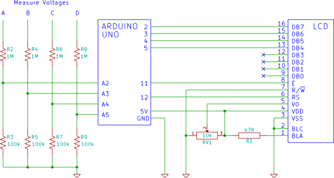
An Arduino voltmeter that displays voltage on an LCD display. The voltmeter has 4 channels for measuring four different voltages. The Arduino voltmeter utilizes an Arduino microcontroller to measure and display voltage levels on a Liquid Crystal Display (LCD). This...
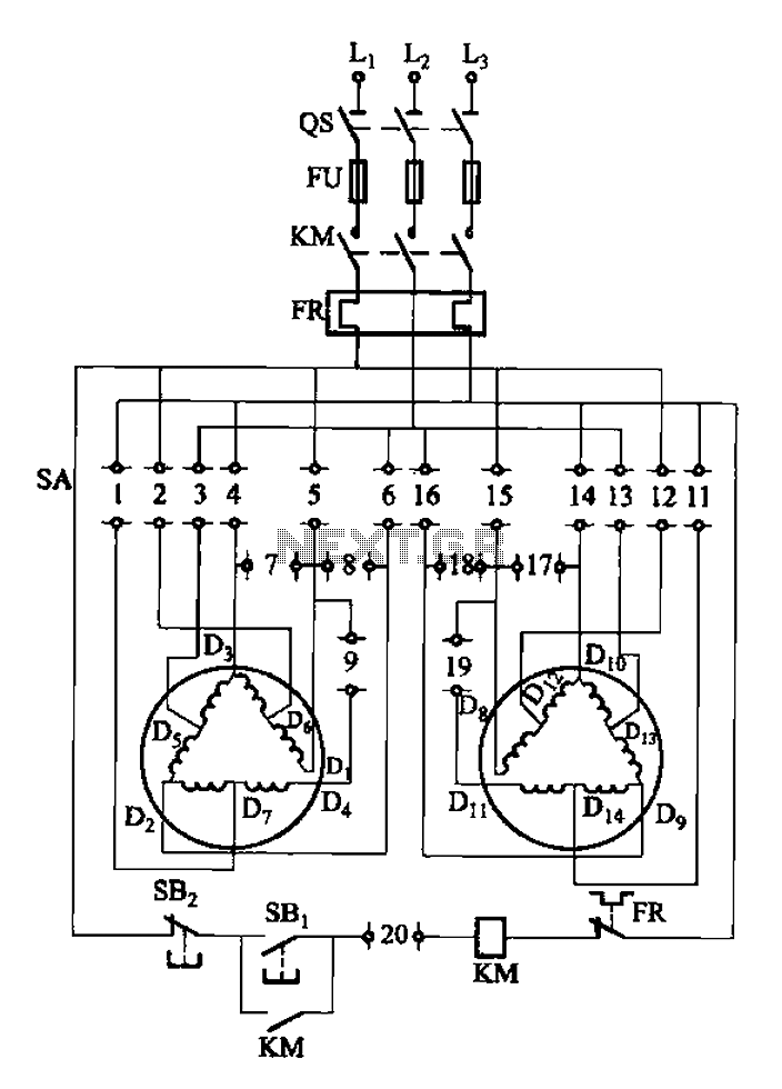
The 3-119 circuit shown in the figure combines switch SA to realize the stator windings, specifically the 2, Y, and 2Y connections, which correspond to the motor speed n1. The 3-119 circuit is designed to facilitate the control of motor...
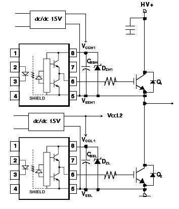
An H-bridge circuit has been developed utilizing four floating gate drivers and four insulated gate bipolar transistors (IGBTs). The attached schematic illustrates one half of the H-bridge configuration. The circuit operates effectively, but there are additional considerations to address. The...
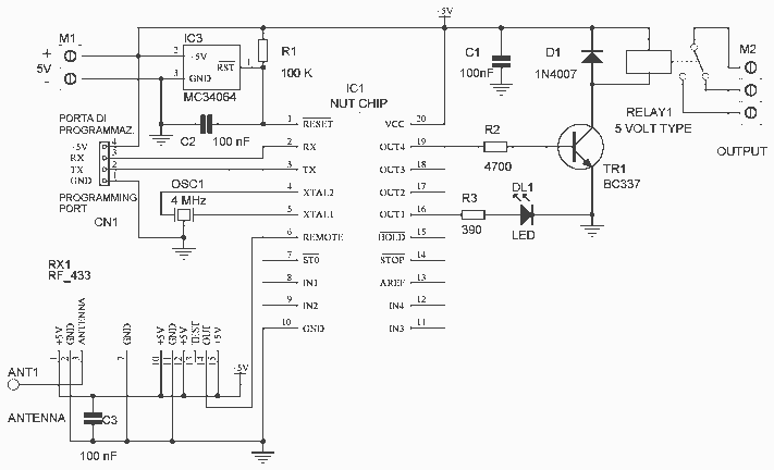
In this project, we will see how to build a single-channel remote control. It is an easy project to do: by using a pre-assembled radio module, we will get a compact card without sacrificing major performance. The insert function...
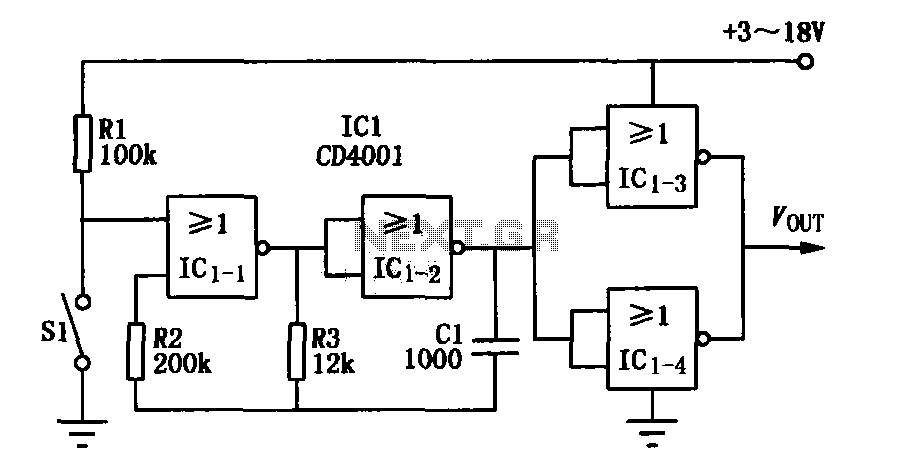
The core elements of this circuit are the second four-input NOR gate terminal IC CD4001. The entire circuit features a simple structure, with fewer components, making it easy to construct, particularly for remote control transmitters or carrier modulation transmission....
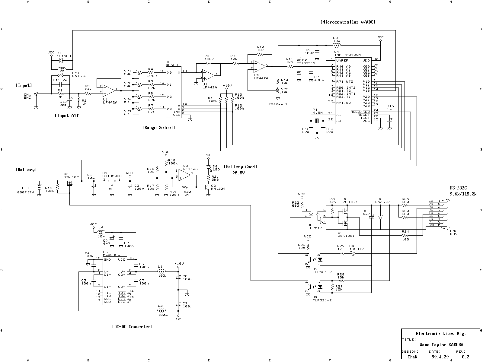
This is a portable oscilloscope adapter that can be held in a breast pocket. Its operation is only sampling and sending to the host PC. Most of the functions of the oscilloscope are processed by the host PC. Therefore,...