
FOUR INPUT VIDEO MIXER

The circuit for combining four positive-polarity marker pulses is essential in radar systems to ensure accurate signal processing and synchronization. The design typically employs a series of resistors and capacitors to manage the timing and amplitude of the incoming pulses. Each marker pulse is generated by separate components, which may include oscillators or pulse generators, and is then fed into a summing circuit.
The summing circuit could utilize operational amplifiers (op-amps) configured in a summing amplifier arrangement. This configuration allows for the integration of multiple input signals while maintaining the integrity of the positive-polarity characteristics. The use of feedback resistors in the op-amp circuit ensures that the output pulse maintains the desired amplitude and shape, suitable for further processing stages in the radar system.
Additionally, the circuit may include filters to eliminate any unwanted noise or interference that could affect the clarity of the combined markers. Proper grounding and shielding techniques are also crucial in radar applications to prevent electromagnetic interference from degrading the performance of the marker pulses.
In summary, the circuit's design focuses on effectively combining multiple positive-polarity marker pulses while ensuring stability and fidelity of the signals within the radar system. This functionality is vital for the accurate operation and performance of radar equipment in various applications.Used for combining four different positive-polarity marker pulses in radar system. -NBS, "Handbook Preferred Circuits Navy Aeronautical Electronic Equipment, " Vol. 1, Electron Tube Circuits, 1963, p N4-1. 🔗 External reference
Related Circuits
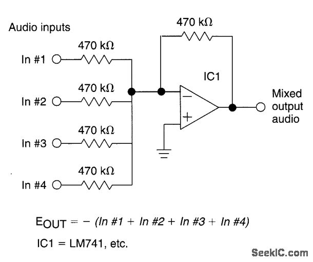
The circuit features four inputs. The voltage gain between each input and the output is maintained at unity by the relative values of the 470kΩ input resistor and the 470kΩ feedback resistor. The described circuit operates as a voltage buffer...
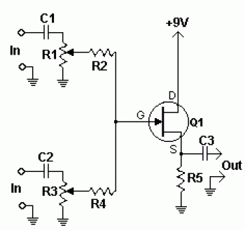
The 2N3819 is an n-channel JFET specifically designed for RF and mixer applications, offering very low noise, minimal distortion, and excellent high-frequency gain. Creating a PCB can be accomplished in a few straightforward steps. Begin by using PCB design...
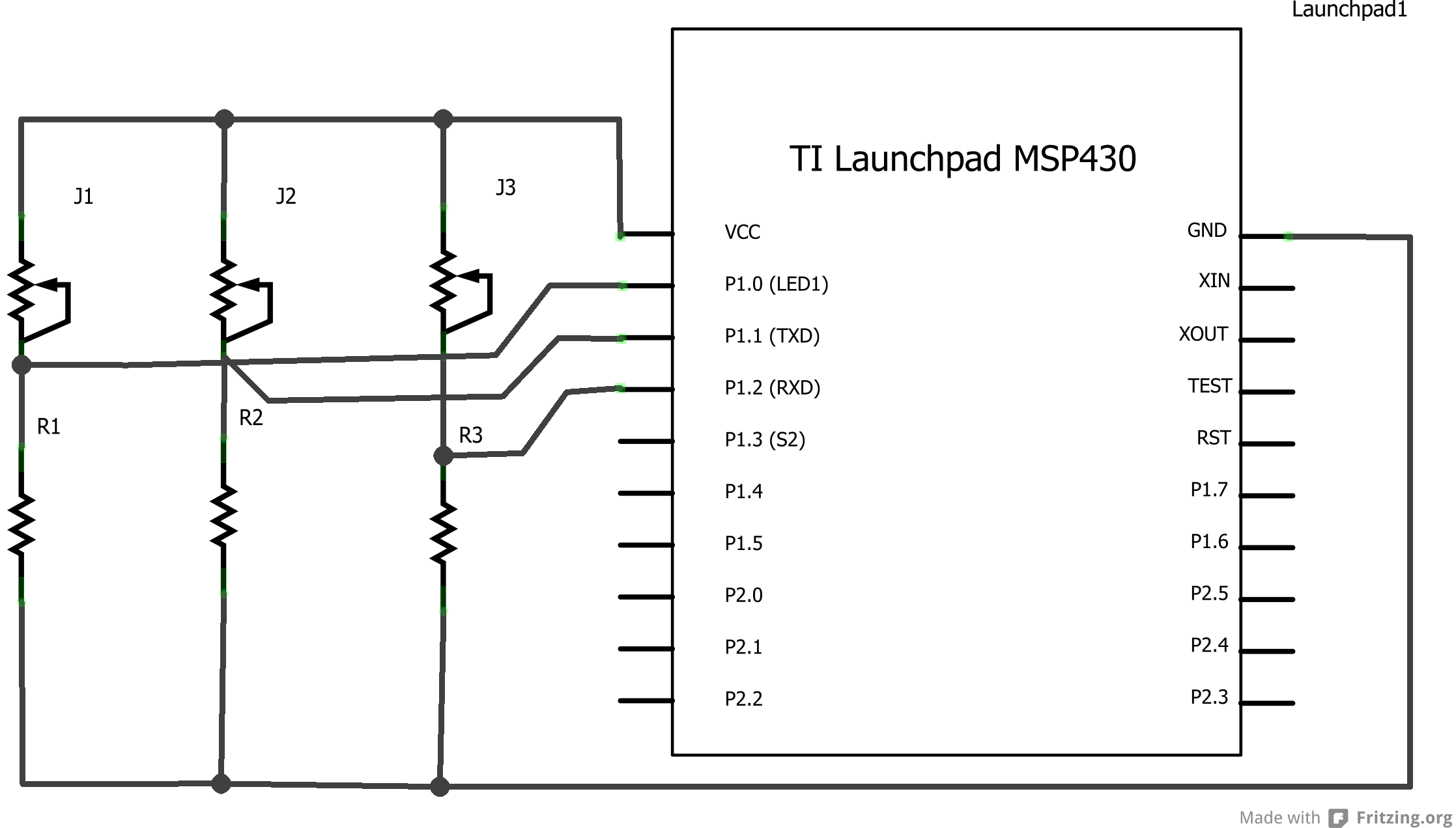
Energia is a rapid prototyping platform designed for the Texas Instruments MCU Launchpad. It is built on the principles of Wiring and Arduino and utilizes the Processing IDE. Energia offers an accessible environment for developing applications with Texas Instruments microcontrollers. By...

Common mode input voltage up to a difference of 100V enlarged circuit diagram. The circuit diagram described features a design capable of handling a common mode input voltage with a differential range of up to 100V. Such a configuration is...
A buffered video amplifier is utilized to connect a video player to a receiver or monitor TV over long cable lengths, which may lead to a reduction in signal amplitude and, consequently, a decline in image quality. This amplifier...
A video digitizer, also known as a frame grabber, captures still picture frames from a television set, video camera, or video recorder, and transmits them to a computer for display, storage, or manipulation. This document outlines the Mark II...