
Frequency Multipliers
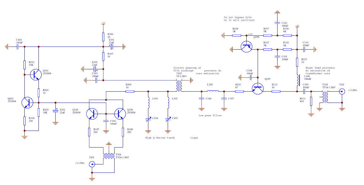
The described circuit employs a pair of JFETs (J1 and J2) to facilitate frequency doubling, specifically utilizing J310, U310, or U431 devices. The biasing resistor R2 is critical for establishing a small drain current under no RF conditions, which aids in maintaining linearity and stability of the FETs during operation. The input transformer (L1) is designed with a specific turns ratio to ensure a 50-ohm impedance match, optimizing power transfer and minimizing reflections.
In terms of performance at UHF frequencies, the circuit benefits from the use of JFETs with higher Idss values and lower capacitance, which are essential for maintaining efficiency and reducing losses. The substitution of Guanella baluns for transformers enhances frequency response and allows for better handling of high-frequency signals.
The LTSpice simulation results provide insight into the operational characteristics of the circuit, revealing a rectified sine wave current profile with a DC offset. This waveform behavior is indicative of the frequency doubling action, where the JFETs switch at twice the input frequency, producing a second harmonic output. The phase noise characteristics are notably improved through careful design choices, such as the inclusion of emitter degeneration in the BJT frequency doubler, which mitigates the effects of noise and instability.
To further refine the output signal, the incorporation of low-pass filters and high Q tuned circuits is essential. These components work collectively to filter out unwanted harmonics and maintain signal integrity at the desired output frequency. The design is particularly sensitive to load impedance, with a specified optimal load of 50 ohms to prevent saturation of the transistors, ensuring consistent performance across varying operating conditions. Overall, the circuit is engineered for high efficiency and low phase noise, making it suitable for applications requiring reliable frequency doubling at UHF frequencies.J1 And J2 are a matched pair of J310`s (can also use U310`s or a U431 matched pair). R2 is selected to bias the 2 FETs with a small drain current with no RF input. The turns ratio of the input transformer is selected for an approximate 50 ohm impedance match at the transformer primary (L1). The combined drain current waveform is a rectified sinewave superimposed on a small dc offset (see below).
At UHF it is desirable to reduce the drain load impedance and the impedance seen by the JFET sources, thus higher Idss low capacitance JFETs are required. Higher frequency operation is possible if Guanella baluns are substituted for the input and output transformers.
N. B. for clarity no parasitic suppression components are shown in the schematic. As shown in the (LTSpice) simulated waveforms shown above the drain current waveform is a rectified sinewave with a small dc current superimposed. There is also a small predominantly 2nd harmonic component of drain current flows via the drain gate capacitance of the JFET.
This is particularly evident when the source current of each JFET is cutoff. NB the JFETS perform the frequency doubling principally by switching action and not due to the JFET square law input characteristic. The output frequency spectrum of the doubler for a 10MHz +13dBm input as seen at the load is displayed below (reference level is 1V rms).
The output level of the frequency doubled component (20MHz)is slightly more than +13dBm. The low phase noise common base BJT frequency doubler shown above is capable of very good performance despite the fact that it uses inexpensive transistors. The low dc gain from base to collector of the dual transistor coupled with the emitter degeneration ensures low phase noise.
The circuit is intended for use with 5MHz or 10MHz input frequencies. Like all frequency doublers it has lowest output phase noise with higher input signals. it is designed for an input of +13dBm and is intended to drive a 50 ohm load (higher load impedances may cause the transistors to enter saturation). The combined collector current waveform is a rectified sinewave superimposed on a small dc offset. Lowest signal phase instability is obtained when a low pass filter with low phase shift at the desired output frequency(2f) is combined with relatively high Q series tuned circuits connected between the common collectors and ground.
These tuned circuits suppress the unwanted frequency components in the output (fundamental (f) 3f, 4f etc). The components at f, 3f, 5f etc are due to inevitable transistor and transformer mismatches, however they will have relatively low amplitudes.
The high Q series resonant (at f, 3f, 5f etc) tuned circuits will contribute little phase shift and associated instability at the desired 2f output frequency. 🔗 External reference
Related Circuits
The simple circuit does not provide isolation; however, its simplicity, combined with the affordability of sound cards and the protective features added by diodes 1 and 2, makes it suitable for the average user. The physical hardware includes a...

When designing bass reflex loudspeaker cabinets, it is essential to measure the speaker's resonance with an accuracy of approximately 1%. This requires an audio oscillator and a frequency counter. However, the accuracy and resolution of a frequency counter when...
Ultrasonic cleaning primarily relies on the phenomenon of ultrasonic cavitation. In the presence of a sound field, liquid bubbles undergo high-frequency micro-vibrations. When the sound pressure reaches a specific threshold, air bubbles grow rapidly and then collapse suddenly, creating...
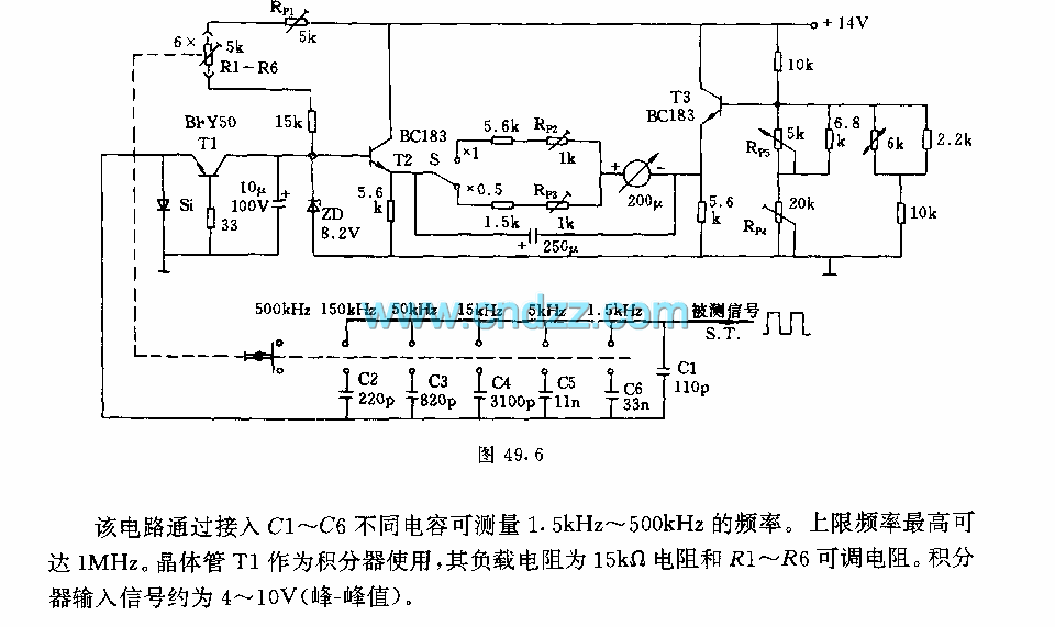
The circuit is capable of measuring frequencies ranging from 1.5 kHz to 500 kHz by connecting different capacitors, C1 to C6. It can handle a maximum frequency of up to 1 MHz. Transistor T1 serves as the integrator, with...
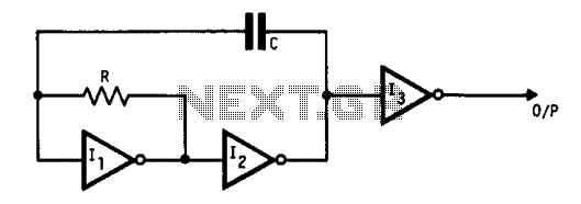
This oscillator utilizes standard inverters, one resistor, and one capacitor, and it does not have a minimum operating frequency. The resistor (R) and capacitor (C) must be selected to ensure that the currents flowing into the gates remain below...
Assistance is required for converting high frequency to low frequency and vice versa. A project involving a sensor is currently in progress, and the schematic is provided below. The conversion of high frequency signals to low frequency signals, as well...