
Low frequency TTL oscillator
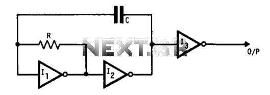
The oscillator circuit described operates based on the principles of feedback and RC timing. The core components include standard inverters, which serve as the primary active elements, along with a resistor and capacitor that establish the timing characteristics. The absence of a minimum operating frequency allows for flexibility in application, making this oscillator suitable for various low-frequency applications.
In terms of component selection, the resistor and capacitor values must be carefully calculated. The resistor value should be chosen to limit the gate current to within safe operating limits specified by the inverter manufacturer. Similarly, the capacitor must be selected to ensure that its leakage current is insignificant compared to the current flowing through the resistor. This is crucial for maintaining stable operation and ensuring that the oscillator functions correctly.
Buffering the output is an essential design consideration. By using a buffer, any variations in the load connected to the oscillator output will not influence the frequency of oscillation. This buffering stage isolates the oscillator from load effects, thereby enhancing the stability and reliability of the circuit.
Furthermore, the circuit's versatility extends to its ability to square up slowly changing logic levels. By incorporating multi-input gates such as NANDs and NORs, the circuit can effectively transform gradual voltage transitions into sharp square wave outputs. This feature is particularly useful in digital applications where clean logic levels are required for reliable operation.
Overall, this oscillator circuit is a simple yet effective design that leverages standard components to achieve reliable oscillation and signal conditioning, making it suitable for various electronic applications.This oscillator uses standard inverters, one resistor and one capacitor, and has no minimum operating frequency. R and C must be chosen such that currents into the gates are below recommended operating limits and that leakage current into the gates and into C are small in comparison with the current in R also the output should be buffered (13) to prevent variations in load affecting frequency.
This circuit may also be used to square up slowly changing logic levels by use.of multi input gates (NANDS, NORS Etc). 🔗 External reference
Related Circuits
A crystal oscillator, particularly a low-frequency variant, can be effectively constructed using an operational amplifier (op-amp) as the amplification component. Below is the schematic diagram of this circuit. The crystal oscillator circuit utilizes the properties of a quartz crystal to...
Under optimal battery conditions, the LED remains off. As the battery voltage decreases, the LED starts to flash, and when the battery reaches a low voltage condition, the LED illuminates continuously. This circuit is designed for use with a...
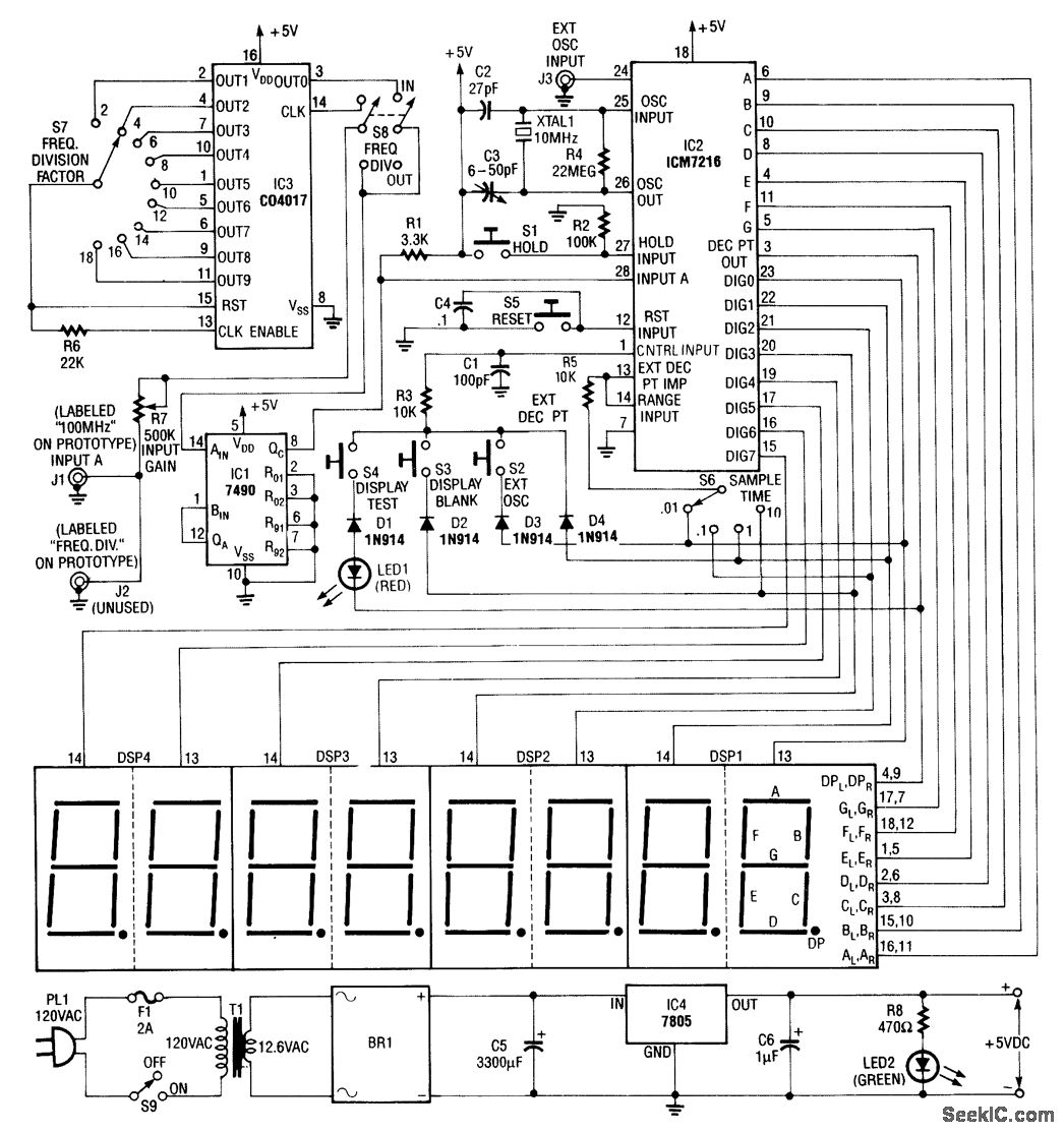
Built around an Intersil 7216 frequency-counter IC, this counter features a basic frequency range of 10 MHz, complemented by a 100-MHz prescaler and an additional frequency divider (IC3). This divider further extends the counting range by dividing the frequency...
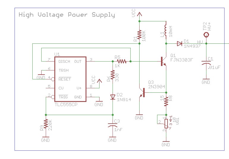
The design involves using a 555 timer as an oscillator in the high voltage power supply section. There is a query regarding the possibility of altering the design to utilize an output from a microcontroller to generate an oscillating...
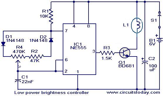
The circuit presented here is designed to control the brightness of low-power incandescent lamps. It utilizes the NE555 integrated circuit, configured as an astable multivibrator with a variable duty cycle. The output from the IC is connected to the...
A display tube utilizing a constant current circuit to ensure a steady flow through the tube. The display tube operates on the principle of maintaining a constant current to achieve consistent brightness and performance. The circuit typically comprises a current...