
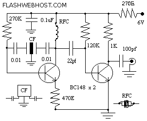
Frequency Shift Keyer

The described circuit utilizes a differential amplifier configuration to achieve signal selection based on the gate voltage level. In this configuration, the differential amplifier has two input channels: channel A and channel B, associated with pins 5, 6 and pins 3, 4, respectively. The operation of the circuit is contingent upon the voltage level present at the gate input (pin 2).
When the gate voltage is set to a high level of 1.5 V, the circuit is designed to allow the signal from channel A (pins 5 and 6) to pass through while simultaneously suppressing the signal from channel B (pins 3 and 4). This selective signal processing enables the circuit to effectively switch between two input signals based on the gate voltage, facilitating the conversion of a binary input into a frequency output.
The binary-to-frequency conversion is directly influenced by the binary sequence applied to the gate input. As the binary sequence changes, the gate voltage transitions between its high and low states, causing the circuit to alternate the output signal between the two channels. This results in a frequency output that corresponds to the binary input sequence, making the circuit suitable for applications in digital signal processing, communication systems, and data encoding.
In summary, the described differential amplifier circuit provides a means to convert binary signals into frequency outputs through controlled signal selection based on gate voltage levels, enhancing its utility in various electronic applications. Apply a signal to each differential amplifier input pair. When the gate voltage is changed from one extreme to the ot her, the output can be switched alternately between the two input signals. When the gate level is high (1.5 V), a signal applied between pins 5 and 6 (channel A) will be passed and a signal applied between pins 3 and 4 (channel B) will be suppressed. In this manner, a binary-to-frequency conversion is obtained that is directly related to the binary sequence, which is driving the gate input (pin 2).
Related Circuits
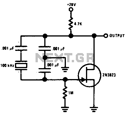
This Colpitts crystal oscillator is ideal for low-frequency crystal oscillator circuits. Excellent stability is assured because the 2N3823 JFET circuit loading does not vary with temperature. The Colpitts crystal oscillator is a type of electronic oscillator that utilizes a combination...
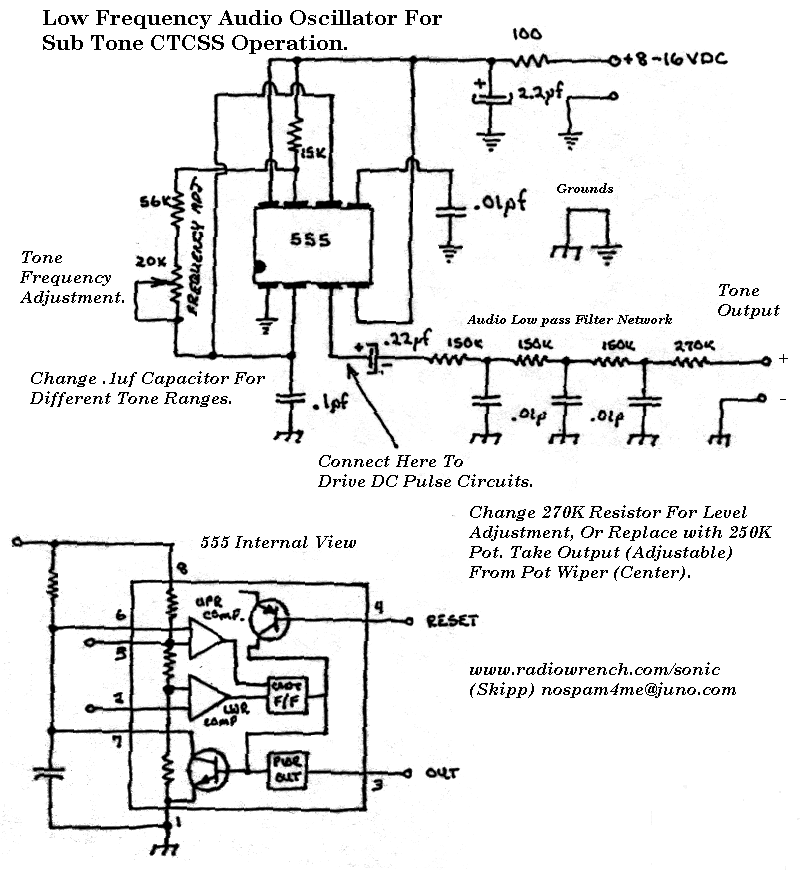
The lf555afosc1.pdf file download contains a diagram with annotations for a Sub-Tone (CTCSS or "PL") Oscillator, designed using the well-known 555 timer IC configured for astable multivibrator operation. The component values are selected to position the tone range near...
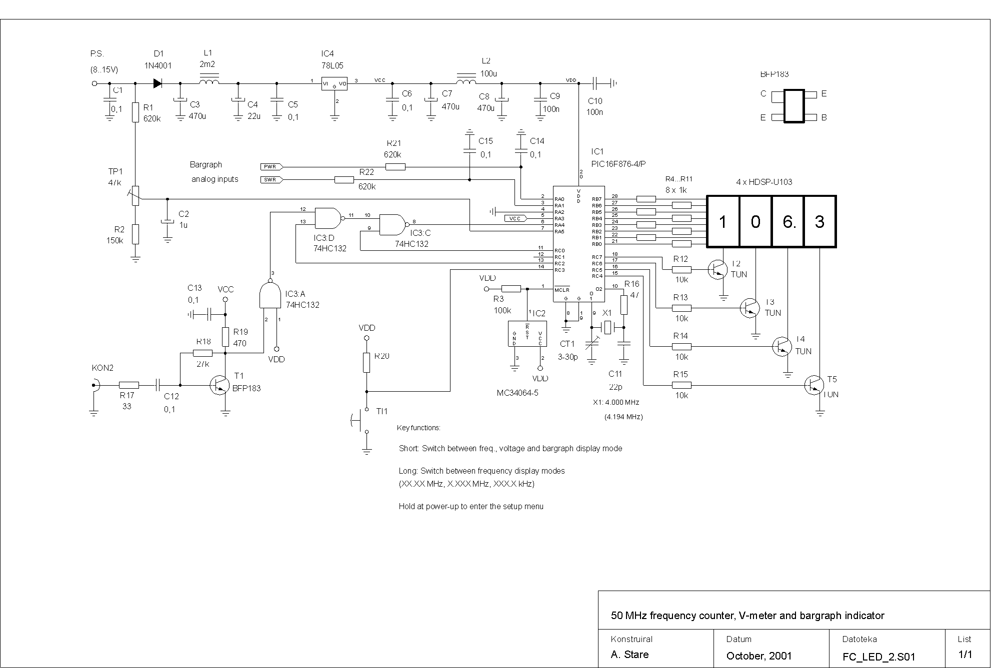
This device is a successor to the PIC16C71 4-digit LED frequency counter and voltmeter. It omits some hard-to-find components from the previous version that have been out of production for some time. The earlier PIC16C71 has been replaced with...
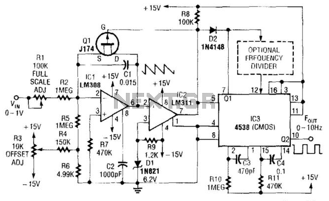
In this circuit, capacitor CI is charged to a fixed reference level and then discharged. The integrator IC1 charges CI until IC1 has a -6.2 V output, at which point comparator IC2 outputs a low signal. FET Q1 triggers...
BFO is a simple device which helps us to listen SSB and CW transmissions. Reception of SSB and CW signals requires a product detector or BFO (Beat Frequency Oscillator) to reinsert the missing carrier. This circuit is very simple...
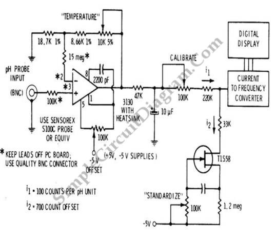
A signal conditioner for a pH meter probe requires high input impedance. The signal conditioning of the pH meter probe is achieved by incorporating a buffer. The design of a signal conditioner for a pH meter probe is critical for...