
Simple Low-Frequency V/F Converter
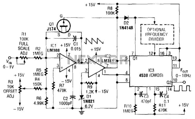
This circuit operates as a timing mechanism utilizing an integrator, comparator, and monostable multivibrator. The primary component, capacitor CI, is charged through a defined pathway until it reaches a threshold voltage of -6.2 V, which is monitored by the comparator IC2. Upon detecting this voltage, IC2 outputs a low signal, which activates the FET Q1. This action triggers one section of the monostable multivibrator IC3, resulting in a brief low state on pin 3 for approximately 470 µs. This pulse duration is critical as it ensures that Q1 fully discharges CI, resetting the capacitor for the next cycle.
The second section of IC3 is configured to generate a longer output pulse, typically around 47 ms. This extended pulse duration allows for stable output signals necessary for applications requiring precise timing. The circuit is designed to operate effectively at a full scale of 10 Hz, which establishes a baseline frequency for the output pulse generation. For applications requiring lower pulse rates, a counter circuit can be integrated between the two sections of IC3, allowing for further manipulation of the output frequency.
However, it is essential to recognize a limitation inherent in the design: while Q1 is conducting, CI does not integrate, leading to potential inaccuracies in the output period. The circuit must be optimized to minimize this error to ensure reliable performance. As a result, the application of this circuit is best suited for low-frequency operations, where the timing accuracy can be maintained without significant deviations. Overall, the design encapsulates a straightforward yet effective approach to generating controlled timing pulses within specified frequency ranges. In this circuit, CI is charged to a fixed reference level, then discharged. Integrator ICl circuit charg es CI until ICl has -6.2-V output, when comparator IC2 outputs a low. FET Ql, triggers one-section monostable multivibrator IC3, pulls pin 3 low for 470, ensuring that Ql completely discharges CI. The other section of IC3 produces a longer pulse of about 47 ms. Full scale of this circuit is 10 Hz. For lower output pulse rates, a counter circuit can be inserted between the sections of IC3. Notice that because CI does not integrate while Ql is biased on, this circuit has an error in the output period, which must be as short as possible.
Therefore, the circuit"s use is limited to low frequencies. 🔗 External reference
Related Circuits
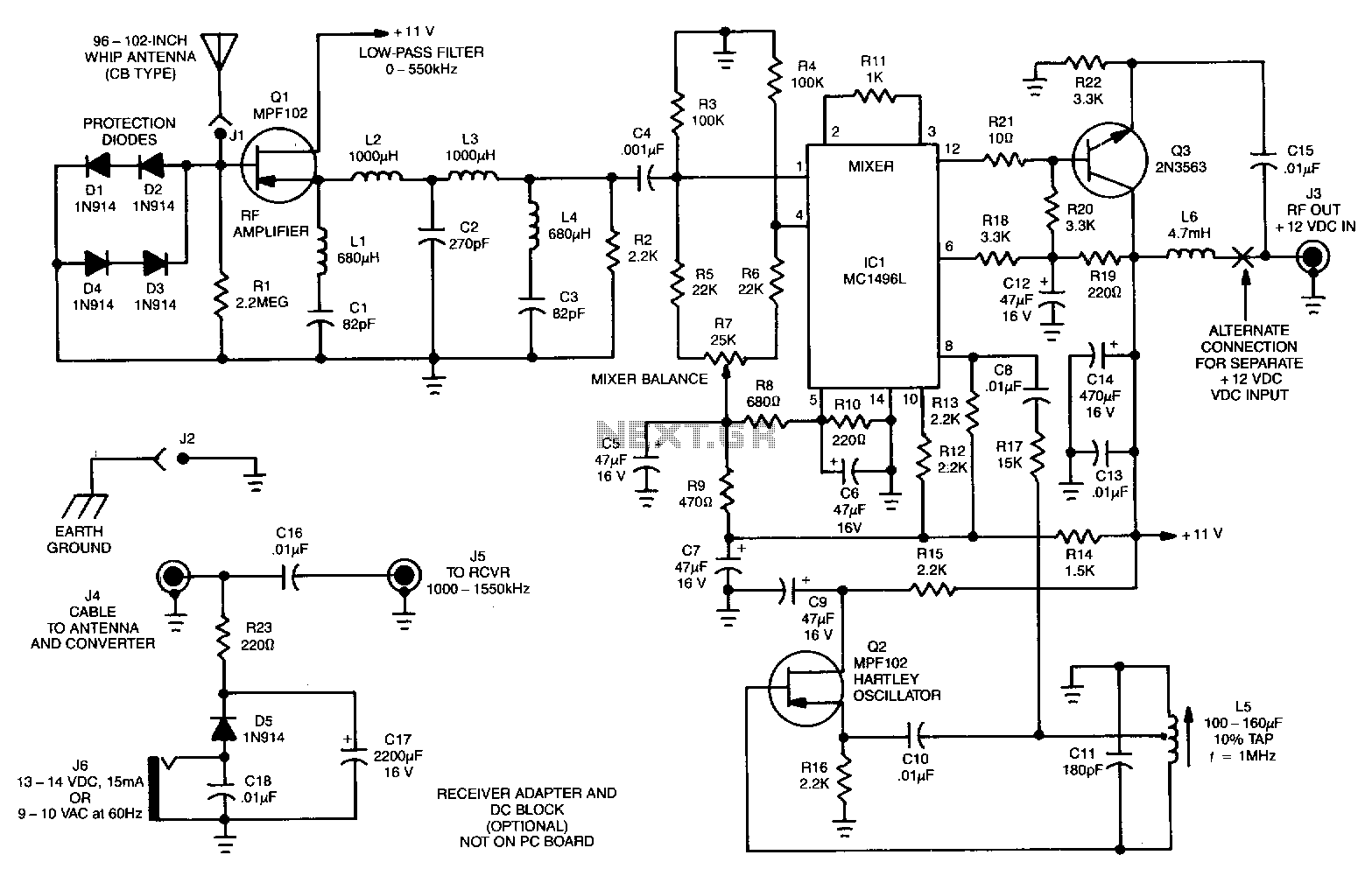
The signals below 550 kHz include maritime mobile, distress signals, radio beacons, aircraft weather information, European Longwave-AM broadcasts, and point-to-point communications. A low-frequency converter transforms the 10 to 500 kHz LW range into a 1010 to 1550 kHz MW...
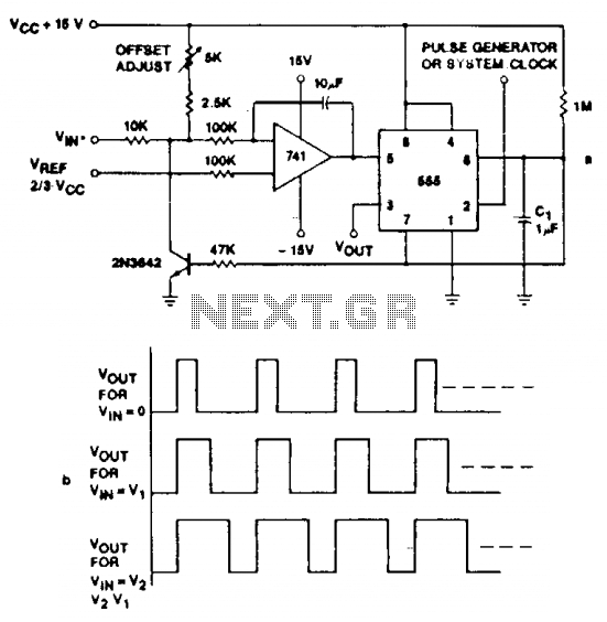
Accuracies better than 1% can be achieved with this circuit (a), and the output signals (b) maintain the original frequency, regardless of the input voltage. Voltage levels can be transformed into pulse durations by integrating an operational amplifier (op...
Most ATV (Amateur Television) transmitters operate using a Double Sideband (DSB) signal, while commercial television stations utilize a Vestigial Sideband (VSB) signal. This distinction is leveraged in this converter to utilize the lower sideband, thereby reducing interference from repeaters...
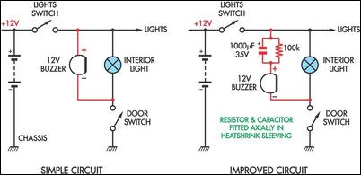
Two headlight reminder circuits are designed for easy installation and operation based on the KISS (Keep It Simple Stupid) principle. The basic circuit consists of a 12V piezo buzzer connected between the lights circuit and a door switch. The...
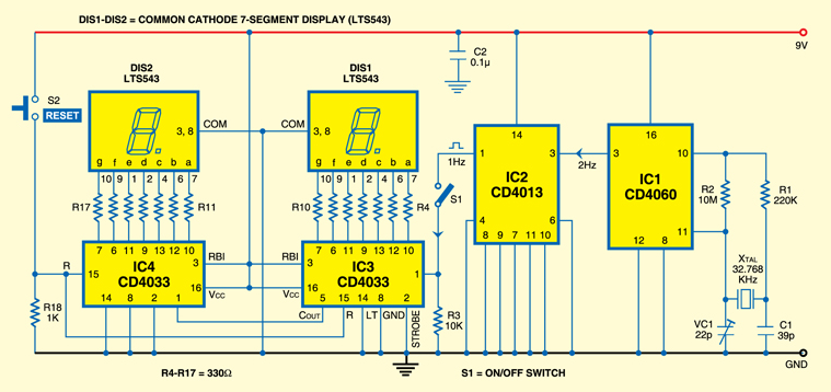
A simple stopwatch circuit that can count up to 99 seconds. The circuit utilizes CD4060, CD4013, CD4033, LTS543, and several discrete components. A crystal-controlled oscillator generates 1Hz pulses using a 32.768kHz miniature crystal. The CD4060 (IC1) features a 14-bit...
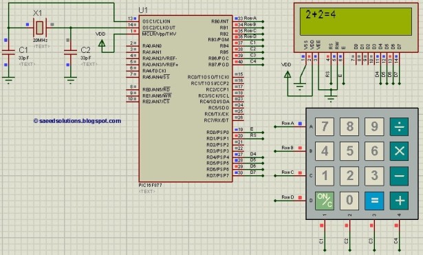
This PIC microcontroller tutorial provides a simple calculator implementation for the PIC16F877 microcontroller. This is a straightforward one-digit calculator. The PIC16F877 microcontroller is a versatile and widely used device in embedded systems, particularly for educational purposes and simple applications. The...
Warning: include(partials/cookie-banner.php): Failed to open stream: Permission denied in /var/www/html/nextgr/view-circuit.php on line 713
Warning: include(): Failed opening 'partials/cookie-banner.php' for inclusion (include_path='.:/usr/share/php') in /var/www/html/nextgr/view-circuit.php on line 713