
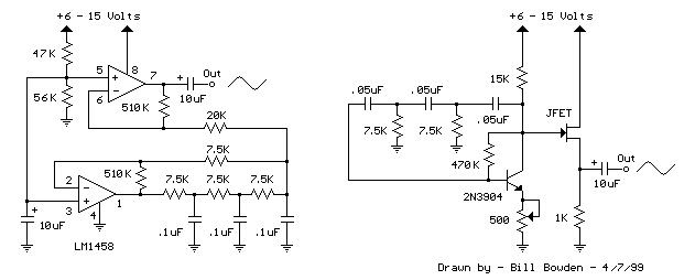
Frequency tripler
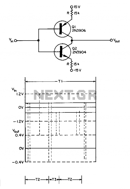
The primary function of this circuit is to utilize the switching characteristics of complementary transistors, typically a PNP and an NPN transistor, to achieve frequency tripling. The design leverages the unique turn-on and turn-off behavior of the transistors to manipulate the input waveform effectively. When a periodic signal is applied, the transistors alternately saturate and cut off, resulting in the generation of additional peaks in the output waveform.
The circuit can be visualized as having an input stage where the periodic waveform is fed into the base terminals of the transistors. As the input signal rises, one transistor turns on while the other turns off, allowing current to flow through the collector-emitter path. This action creates a corresponding output peak. When the input signal reaches a certain threshold, the first transistor saturates, causing the second transistor to turn on, which generates the second output peak. This process continues, resulting in the tripling of the frequency of the original input signal.
The output waveform will contain three distinct peaks for every cycle of the input waveform, effectively tripling the frequency. However, the circuit's performance may be compromised by the asymmetry of the output peaks, which can lead to distortion in the final signal. This lack of symmetry arises from the inherent differences in the turn-on and turn-off times of the complementary transistors, which can be influenced by factors such as transistor characteristics and circuit design.
This circuit's operational frequency range extends from DC up to the maximum frequency that the selected complementary transistor pair can handle, making it versatile for various applications in signal processing. The design can be further optimized by selecting transistors with matched characteristics to minimize output asymmetry and improve overall performance.The turn-on and turn-off characteristics of two complementary transistors can be combined to attain nonselective frequency tripling. The resulting circuit handles any periodic waveform with nonvertical sides. Each input signal peak produces three output signal peaks. The additional peaks occur where the input signal causes saturation of one of the two transistors. The circuit operates over a frequency range from dc to the upper limits of the complementary transistor pair.
About the only disadvantage of the circuit is the lack of symmetry of the output signal peaks. 🔗 External reference
Related Circuits
Spikes in the center of a sawtooth wave are eliminated in this circuit by triggering at specific intervals. This circuit is designed to mitigate unwanted spikes that occur in the center of a sawtooth waveform. The sawtooth wave, characterized by...
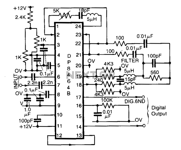
The DP8464B from National Semiconductor is designed primarily for use in disk systems as a pulse detector. However, it can also function effectively as a general-purpose peak detector for analog signals up to 5 MHz. This integrated circuit can...
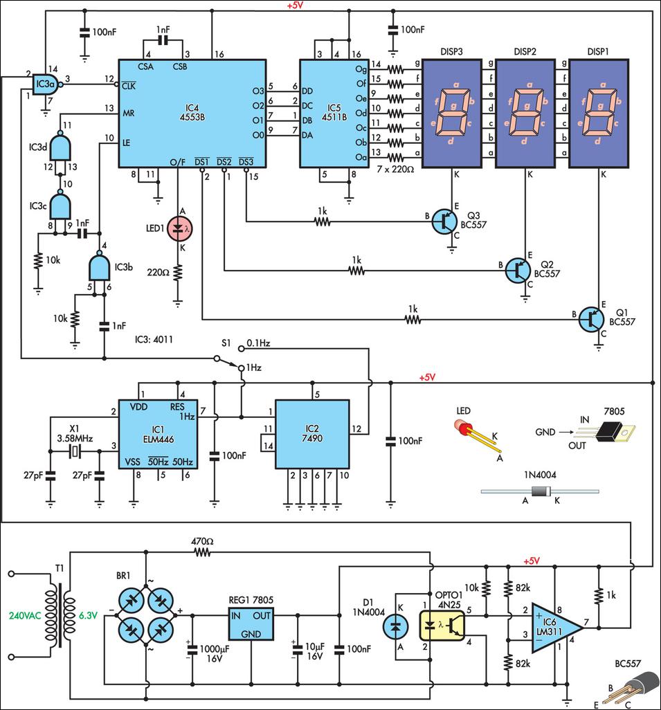
This is a simple frequency counter designed to monitor the 240VAC mains supply. It has a frequency range of 0-999Hz, making it suitable for use with 400Hz equipment as well. Standard TTL/CMOS logic is utilized for the counters and...
The two circuits below illustrate the generation of low-frequency sine waves by shifting the phase of the signal through an RC network, ensuring that oscillation occurs when the total phase shift reaches 360 degrees. The transistor circuit on the...
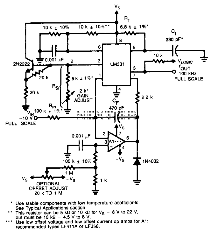
This circuit utilizes a conventional operational amplifier in conjunction with a feedback capacitor (CF) to perform integration. When the output of the integrator exceeds the nominal threshold level at pin 6 of the LM131, it triggers the timing cycle....
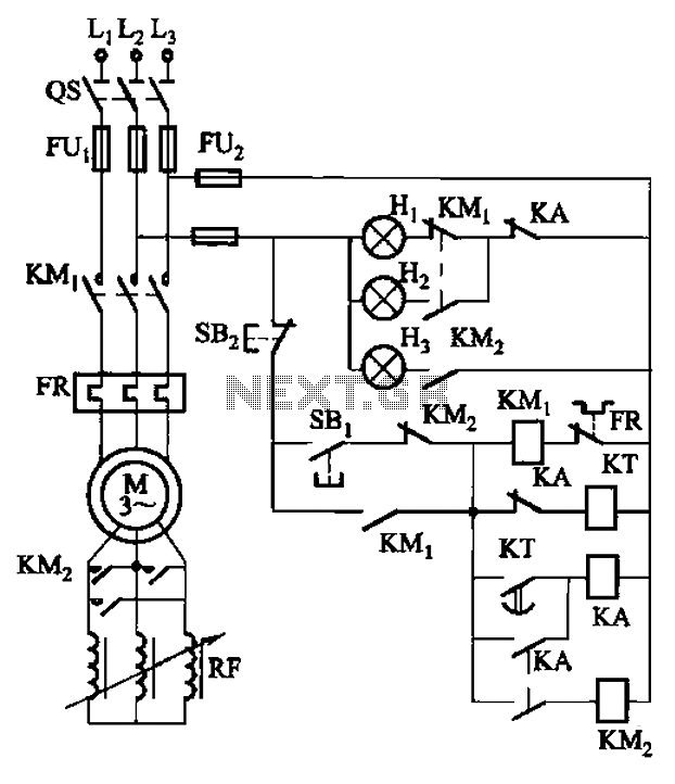
The circuit depicted in Figure 3-165 utilizes a time relay (KT) for controlling the start-up time. Indicator light Hi serves as the power indicator, H2 is designated for the start lights, and H3 functions as the running lights. The circuit...
Warning: include(partials/cookie-banner.php): Failed to open stream: Permission denied in /var/www/html/nextgr/view-circuit.php on line 713
Warning: include(): Failed opening 'partials/cookie-banner.php' for inclusion (include_path='.:/usr/share/php') in /var/www/html/nextgr/view-circuit.php on line 713