
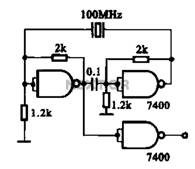
FT0 frequency synthesizer circuit

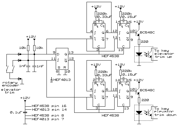
The circuit described involves a frequency synthesizer, which is a crucial component in various electronic applications, including telecommunications and signal processing. The D flip-flop serves as a fundamental building block for the synthesizer, enabling the generation of stable frequency signals through its ability to store and transfer binary data.
In this configuration, the D flip-flop operates with two primary control inputs: the SET (S) and RESET (R) pins. When the SET pin is activated, the output Q is driven high (logic level 1), while the complementary output Q' is driven low (logic level 0). Conversely, activating the RESET pin forces the output Q to low (logic level 0) and Q' to high (logic level 1). This functionality is essential for initializing the state of the flip-flop and for synchronizing the output with the clock signal utilized in the frequency synthesizer.
The connections to VDD and VSS are critical for providing the necessary power supply to the flip-flop. VDD (pin 9) typically connects to the positive supply voltage, ensuring that the logic levels are properly defined, while VSS (pin 8) connects to ground, establishing a common reference point for the circuit. The link from pin 12 to the phase comparator 2 indicates that the output of the D flip-flop is used as an input to the phase comparator, which likely plays a role in maintaining phase-locked loop (PLL) functionality within the synthesizer.
In summary, the D flip-flop, represented by components such as the 74LS74 in TTL or the CD4013 in CMOS, is integral to the frequency synthesizer circuit. Its ability to store binary data and provide controlled output states is essential for achieving the desired frequency output and maintaining synchronization within the overall circuit design.I m planning to construct a frequency synthesizer circuit and i found this circuit diagram..but i m unable to figure out a component..can any1 explain 2me what is the part with the VDD from pin 9,Vss from pin 8 and pin 12 connected to the phase comparator 2 It is a simple 'D' type data latch with SET and RESET. If you search through enough CMOS data sheets you can probably identify which one. that is a D flip flop with set and reset pin D=vdd it is an input bit R=reset S=set Q=state 1 Q'=state2 Q and Q' are outputs it inverted output to each other if Q=1 then Q' is zero and vice-versa in TTL it may be a 74LS74 in CMOS it may be a CD4013 🔗 External reference
Related Circuits
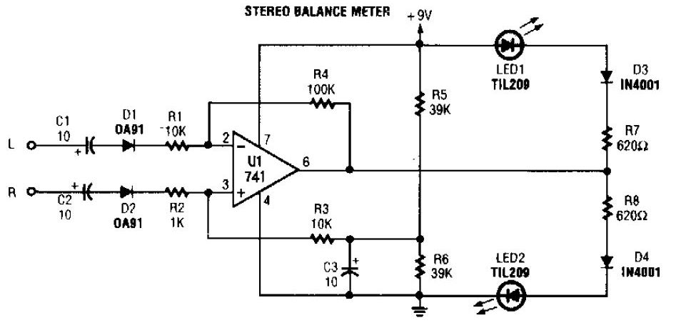
The simplest stereo balance meter circuit schematic available on the internet. When the left and right signals are equal, no output is present from U1 and pin. This stereo balance meter circuit is designed to visually indicate the balance between...
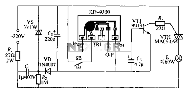
The circuit utilizes a KD-9300 music IC, which activates when the button switch (SB) is pressed, causing the electric lamp (E) to light up for approximately 20 seconds before automatically turning off. The setup includes a half-wave rectifier and...
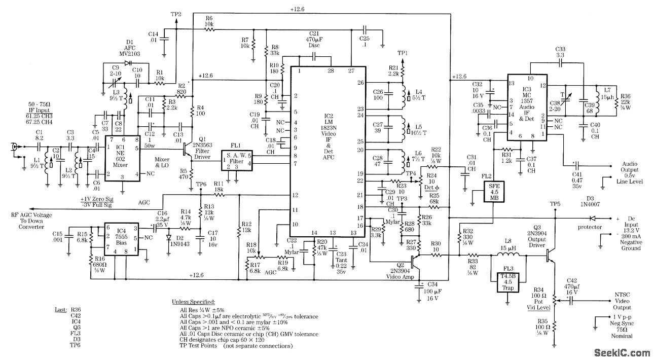
Radio-frequency schematics (also see NE602 datasheet and application note). This page contains electronic circuits related to RF receivers. This index features a broad collection of RF receiver circuits. Radio-frequency (RF) schematics are essential for designing and implementing circuits that operate...
Crystal oscillator integrated circuits, specifically two diagrams of oscillator circuits with oscillation frequencies of 10 MHz and 20 MHz. Crystal oscillators are essential components in various electronic applications, providing stable frequency references for timing and synchronization purposes. The circuits presented...
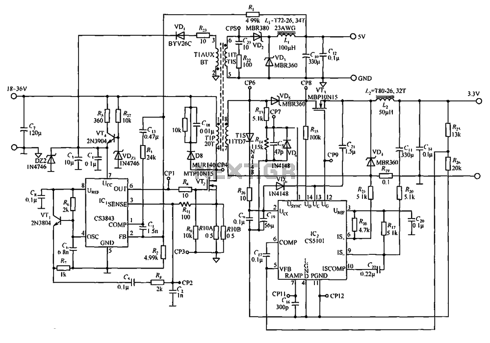
The CS3843 and CS5101 are components of a 5V/3.3V switching DC power supply circuit. The CS3843 is a fixed frequency PWM controller characterized by a set oscillator that precisely controls the duty cycle. It features a temperature-compensated reference voltage,...
After conducting experiments with a rotary encoder connected directly to keyboard switches, it was found that the keyboard controller IC (an Intel P8049AH in this case) is unable to detect pulses that are too narrow. Testing involved rotating the...