
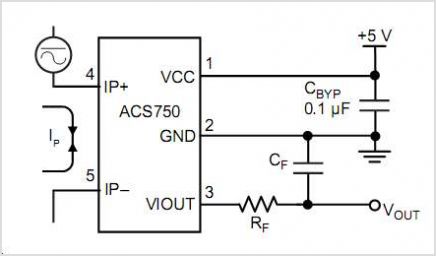
Fully Integrated Hall Effect-Based Linear Current Sensor With High Voltage Isolation And A Low-Resistance Current Conductor
The AD537 voltage-to-frequency converter is designed for high precision applications where converting voltage signals into frequency signals is essential. The internal architecture includes a high-performance input amplifier that ensures low drift and high input impedance, making it suitable for interfacing with low-level signals from sensors such as thermocouples or strain gauges. The precision oscillator system generates a stable frequency output that is proportional to the input voltage, allowing for accurate signal conversion across a wide frequency range.
The device's ability to operate with a single supply voltage simplifies the design of power supply circuits, and the low quiescent current of 1.2 mA contributes to energy efficiency, making the AD537 ideal for battery-operated devices. The temperature-proportional output enhances its utility in temperature measurement applications, enabling easy integration with temperature control systems.
The output characteristics of the AD537 are particularly advantageous, as the square-wave output can drive multiple TTL loads, making it suitable for interfacing with digital circuits and microcontrollers. The robust construction, featuring hermetically sealed packages, ensures reliability in harsh environments, while the availability of different performance grades allows for flexibility in selecting the appropriate version based on the application's temperature requirements.
In summary, the AD537 is a versatile and reliable voltage-to-frequency converter that combines high accuracy, low power consumption, and excellent temperature stability, making it an ideal choice for a wide range of electronic applications.The AD537 is a monolithic V-F converter consisting of an input Amplifier a precision Oscillator system, an accurate internal reference generator and a high current output stage. Only a single external RC network is required to set up any full-scale (F. S. ) frequency up to 100 kHz and any F. S. input voltage up to 30 V. Linearity error is as low as 0 . 05% for 10 kHz F. S. , and operation is guaranteed over an 80 dB dynamic range. The overall temperature coefficient (excluding the effects of external components) is typically 30 ppm/C. The AD537 operates from a single supply of 5 V to 36 V and consumes only 1. 2 mA quiescent current. A temperature-proportional output, scaled to 1. 00 mV/K, enables the circuit to be used as a reliable temperature-to-frequency converter; in combination with the fixed reference output of 1.
00 V, offset scales such as 0C or 0F CAN be generated. The low drift (1V/C typ) input Amplifier allows operation directly from small signals (e. g. , thermocouples or strain gages) while offering a high (250 M(Ohm) input resistance. Unlike most V-F converters, the AD537 provides a square-wave output, and CAN drive up to 12 TTL loads, LEDs very long cables, etc. The excellent temperature characteristics and long-term stability of the AD537 are guaranteed by the primary bandgap reference generator and the low T.
C. silicon chromium thin film resistors used throughout. The device is available in either a TO-116 ceramic DIP or a TO-100 metal can; both are hermetically sealed packages. The AD537 is available in three performance/temperature grades; the J and K grades are specified for operation over the 0C to +70C range while the AD537S is specified for operation over the extended temperature range, -55C to +125C.
*Protected by Patent Nos. 3, 88, 963 and RE 20, 586. 🔗 External reference
Related Circuits
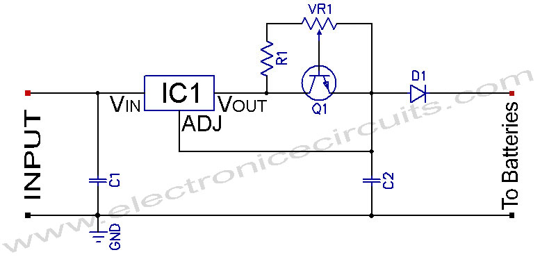
Adjustable Constant Current Ni-Cd and Ni-MH Battery Charger Circuit. This circuit is designed to provide an adjustable constant current for charging Ni-MH or Ni-Cd batteries. The adjustable constant current battery charger circuit is engineered to cater to the specific charging...
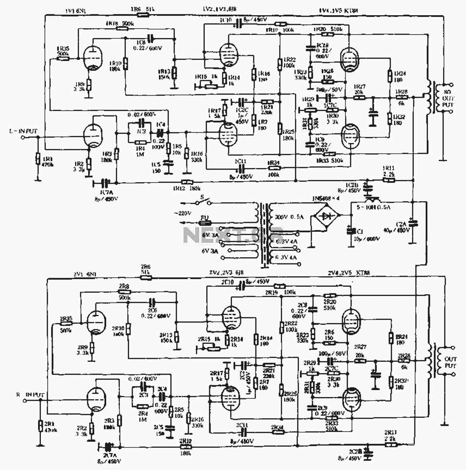
A standard linear amplifier is designed according to a conventional circuit configuration, with the power of the beam tube indicated in Figure 1-8. The output stage employs power tubes such as EL34, KT88, and KT100, which are types of...
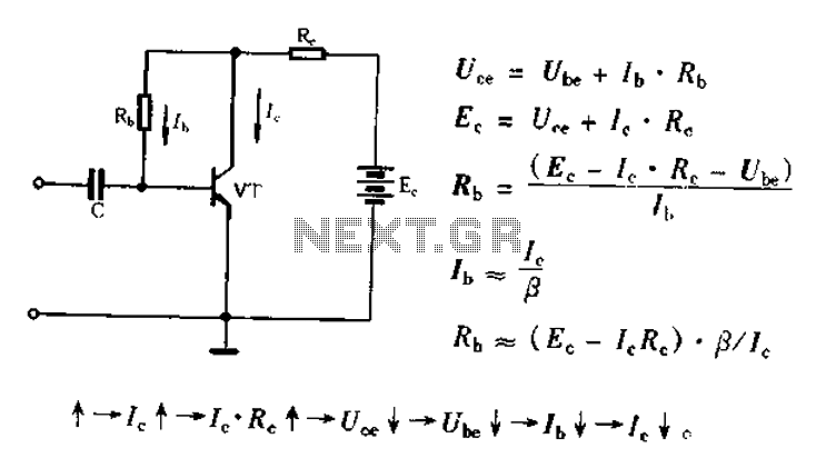
Bias voltage negative feedback circuit The bias voltage negative feedback circuit is a crucial component in various electronic applications, particularly in amplifiers and oscillators. This circuit is designed to stabilize the operating point of a transistor or operational amplifier by...
A DC-to-DC step-up converter is typically implemented using a transformer, which converts DC voltage to AC voltage, steps it up with the transformer, and then rectifies and filters the output to achieve a higher DC voltage. However, a voltage...
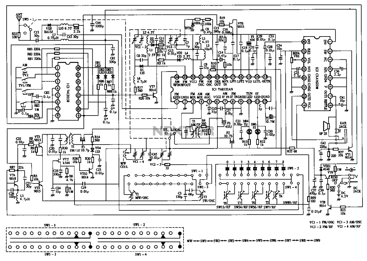
The circuit diagram for the Desheng 119 700 type FM, TV sound, medium wave, and short wave high sensitivity L2-band stereo radio is presented below. The Desheng 119 700 type radio circuit is designed to receive various frequency bands including...
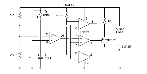
In this circuit, an LM339 quad voltage comparator is utilized to generate a time delay and control a high current output at low voltage. Approximately 5 amps of current can be sourced using a pair of fresh alkaline D...