
GPS Receiver RF Block Diagram Based On The MAX2742 IC

The GPS receiver RF block diagram utilizing the MAX2742 IC encompasses several critical components that facilitate the reception and processing of GPS signals. The MAX2742 is a low-noise amplifier (LNA) designed specifically for GPS applications, offering high gain and low noise figure, which are essential for capturing weak satellite signals.
The RF block typically begins with an antenna designed to receive signals from GPS satellites. The antenna is connected to the input of the MAX2742, where the incoming RF signals are amplified. Following amplification, the signals pass through a bandpass filter to eliminate out-of-band noise and interference, ensuring that only the relevant GPS frequencies are processed.
After filtering, the amplified and cleaned signals are fed into a mixer stage, where they are combined with a local oscillator signal. This process downconverts the RF signals to an intermediate frequency (IF), which is easier to process. The choice of local oscillator frequency is crucial, as it determines the final IF frequency and affects the overall performance of the receiver.
Subsequent stages may include additional filtering, further amplification, and analog-to-digital conversion, allowing the digital signal processing unit to extract position, velocity, and timing information from the GPS signals. The MAX2742's integrated features help streamline the design and reduce the component count, making it an efficient choice for GPS receiver applications.
Overall, the block diagram of the GPS receiver illustrates the fundamental architecture and signal flow necessary for effective satellite navigation, leveraging the capabilities of the MAX2742 to achieve reliable performance in various environments.Description:The following circuit shows about GPS Receiver RF Block Diagram. This circuit based on the MAX2742 IC. Features: a complete GPS receiver, GPS .. 🔗 External reference
Related Circuits
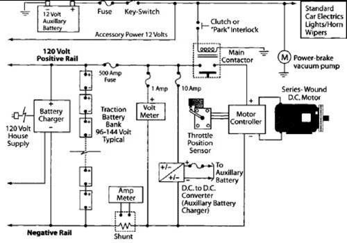
After charging the batteries for many hours with the 12V charger and PowerCheqs, a drive of about 5 miles resulted in the low battery light activating. The PakTrakr indicated that the battery adjacent to the most positive battery required...
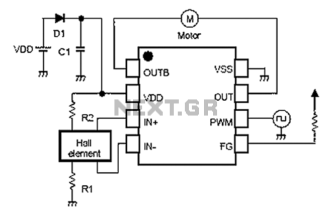
A simple single-phase brushless DC motor drive using the NJU7365 motor driver IC from New Japan Radio Co., Ltd. The NJU7365 is designed for single-phase motor applications and features built-in MOSFET motor drives, direct PWM input, FG output, and...
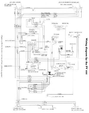
The following circuit illustrates the wiring diagram for the Volvo PV444, a vintage car electrical circuit. It provides an electrical understanding of this uni-body vehicle. The Volvo PV444 wiring diagram serves as a crucial reference for understanding the electrical system...
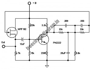
The following circuit illustrates a stable 60 Hz frequency signal generator circuit diagram. Features include a 0.068 µF capacitor incorporated within a feedback loop, allowing for DC-to-AC conversion. This circuit is designed to generate a stable 60 Hz sine wave...

This design features a simple yet effective receiver with good sensitivity and selectivity. The circuit utilizes a compact three-transistor regenerative receiver with fixed feedback, primarily based on the BC549 transistor. The tuned circuit is intended for medium wave frequencies...
A digital amplifier is a new device that IC manufacturers are eager to capitalize on, leading to the launch of unique digital amplifier products. Below are brief descriptions of some representative devices. The TA2022, produced by Tripath, is an...