
Halogen Lamp Dimmer With Soft Start
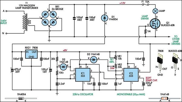
This circuit description outlines a PWM-based dimmer design that effectively manages lamp brightness while addressing the limitations of traditional dimmers, particularly with respect to inductive loads. The use of high-frequency PWM not only enhances performance but also ensures safety through isolation from mains voltage. The dual 555 timer configuration allows for precise control over the timing and output pulses, making it suitable for various applications where adjustable brightness is required. The inclusion of a soft-start feature further contributes to the longevity of the lamp, while the choice of components ensures efficient operation under varying load conditions. Overall, this design exemplifies a robust approach to modern dimming solutions in electronic lighting systems.Most dimmers use pulse width modulation (PWM) to control the amount of power that is delivered to the lamp. Those that come bundled with a switch faceplate control the firing angle of a Triac on the 240V mains side.
These work fine with resistive loads but may not be suitable for inductive loads such as low-voltage halogen lamp transformers. Thiscircuit also employs PWM but it switches at a high frequency (22kHz) on the low-voltage side of the lamp transformer. This high frequency also simplifies EMI filtering. Furthermore, because this circuit is isolated from the mains by the transformer, it is relatively safe to build and install.
IC1 is a standard 555 astable oscillator with a high duty cycle. It produces a narrow negative-going pulse at its pin 3 output approximately every 45 µs (ie, the frequency of oscillation is about 22kHz). These pulses trigger IC2, another 555 timer, this time wired as a variable monostable. IC2`s pin 3 output is normally low which means that its internal discharge transistor is on and the 1nF capacitor on pins 6 & 7 is discharged.
However, when the monostable is triggered (by IC1), its output goes high, the internal discharge transistor turns off and the 1nF capacitor charges via VR1 & VR2 until it reaches 2/3Vcc. At this point, the output at pin 3 switches low again. Each time pin 3 of IC2 goes high, it turns on power Mosfet transistor Q1 which in turn switches on the lamp.
Potentiometer VR2 is used to control the time it takes the 1nF capacitor to charge to the threshold voltage and thus sets the width of the output pulses. At maximum resistance, the pulse width is 55ms. This is longer that the 45ms period of oscillator IC1, and so IC2`s pin 3 output is high for 100% of the time and the lamp operates with maximum brightness.
Now consider what happens if the monostable`s period is shorter than the astable`s. In this case, each time IC1`s pin 3 output goes low, pin 7 of IC1 also goes low and discharges IC2`s 1nF timing capacitor via D3. This retriggers the monostable. As a result, IC2 is triggered at a 22kHz rate and produces variable width pulses depending on the setting of VR2.
It`s output in turn pulses Q1 to control the lamp brightness. D2 isolates IC1`s timing circuitry from IC2`s. VR1 is used to set the minimum lamp brightness when VR2 is at minimum resistance. If this control is not required, VR1 can be replaced with a 1. 8kO resistor. The 220 µF capacitor on pin 5 of IC2 provides a soft-start facility to prolong lamp life. Initially, when power is first applied, the 220 µF capacitor is discharged and this lowers the threshold voltage (which is normally 2/3Vcc). That in turn results in shorter pulses at the output. As the 220 µF capacitor charges, the threshold voltage gradually increases until the circuit operates "normally".
For the prototype, Q1 was a BUK553-60A, rated at 60V, 20A & 75W. Q1`s maximum on-state resistance is 0. 1O, so switching a 4A lamp load results in a maximum power dissipation of 1. 6W. The bridge rectifier comes in at around 5W and so both should be mounted on suitable heatsinks. The power dissipation in the bridge rectifier can be reduced by using power Schottky diodes rated at 5A or more. The output of 555 timer IC2 is capable of directly driving several Mosfets (up to four in tests). Note, that if the Mosfet is going to be some distance from the 555, it will be necessary to buffer it.
Power for the control circuitry is derived from 3-terminal regulator REG1 which produces an 8V rail. This in turn is fed from the output of the bridge rectifier via diode D1 🔗 External reference
Related Circuits
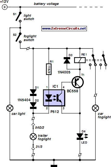
A rear fog lamp is mandatory for trailers and caravans to enhance visibility during foggy conditions. When the fog lamp is activated, the fog lamp of the towing vehicle must be turned off to prevent distracting reflections. To achieve...
Several individuals have encountered difficulties in locating the transformer required for the Black Light project. Consequently, a search was conducted to identify a fluorescent lamp driver that operates without the necessity for specialized components. A suitable option was discovered...

It connects to the USB port and is ideal for checking motherboard switches and jumper settings. Many users may recall a commercial product from a few years ago, the "Itty Bitty Book Light," which was designed to clip onto...
Q1 and Q2 create an ALL-ON ALL-OFF circuit that, when in the off state, draws negligible current. P1 initiates the circuit, activating the relay and powering the two integrated circuits (ICs). The lamp is energized through the relay switch,...
This circuit functions as a low-frequency warning device. The output from the oscillator generates a square wave signal, which is utilized to operate lamps or small relays. The circuit alternately flashes two incandescent lamps. The low-frequency warning device circuit typically...
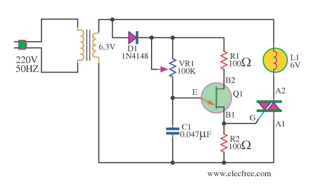
This circuit is an AC dimmer designed for low voltage lamps operating at 6V. While some may not recognize the benefits of this circuit, it serves as an excellent introduction to understanding the operation of a TRIAC. Additionally, it...