
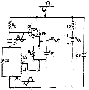
Hartley Oscillator
One variant of the series-fed Hartley oscillator includes a tank circuit comprised of a tapped coil (L1 and L2) and capacitor C2. The feedback circuit connects the tank circuit to the base of transistor Q1 via coupling capacitor C1. This coupling capacitor prevents the low DC resistance of L2 from shorting the emitter-to-base junction and resistor RE. Capacitor C3 bypasses the sine-wave signal around the battery, while resistor RE is implemented for temperature stabilization to avert thermal runaway. Degeneration is mitigated by capacitor CE, which is in parallel with RE. The biasing is determined by the values of RB, the emitter-to-base resistance, the small DC resistance of coil L1, and the resistance of RE. When voltage is applied, current from the battery flows through coil L1 and to the emitter via RE. This current then proceeds from the emitter to the collector and back to the battery. The surge of current through coil L1 induces a voltage in coil L2, initiating oscillations within the tank circuit. Initially, when current flows through coil L1, the bottom of L1 is negative relative to the top of L2, which induces a positive voltage at the top of L2. This positive potential is coupled to the base of Q1 through capacitor C1, enhancing the forward bias of Q1 and increasing the collector current. The rise in collector current also amplifies the emitter current flowing through coil L1, supplying additional energy to the tank circuit, further elevating the positive potential at the top of L2 and increasing Q1's forward bias. This feedback loop continues until the rate of current change through coil L1 reaches a maximum limit, preventing indefinite current increase that could damage the coil and transistor. The circuit must be designed with appropriate component selection to ensure a stable operating point is achieved. When this point is reached, capacitor C2 is charged to the potential across L1 and L2. As the current through L1 begins to decrease, the voltage induced in L2 also drops, leading to a decrease in the positive potential across the tank circuit and causing C2 to discharge through L1 and L2. This discharge maintains current flow through the tapped coil and results in a reduction of Q1's forward bias, subsequently decreasing the collector and emitter currents. When the potential across the tank circuit diminishes to zero, the energy stored is contained within the magnetic field of the coil, completing a half cycle of operation. Following this, the collapsing magnetic field around L2 generates a negative charge at the top of L2 as the current from C2 ceases.
The Hartley oscillator's design allows for flexible frequency generation and tuning, making it suitable for various applications in communication systems and signal processing. Its simplicity and effectiveness in generating stable oscillations make it a valuable component in electronic circuits. The careful selection of components, including transistors and resistors, is crucial to ensure reliable operation and prevent thermal issues, thereby enhancing the overall performance of the oscillator.The HARTLEY OSCILLATOR is an improvement over the Armstrong oscillator. Although its frequency stability is not the best possible of all the oscillators, the Hartley oscillator can generate a wide range of frequencies and is very easy to tune. The Hartley will operate class C with self-bias for ordinary operation. It will operate class A when the output waveform must be of a constant voltage level or of a linear waveshape. The two versions of this oscillator are the series-fed and the shunt-fed. The main difference between the Armstrong and the Hartley oscillators lies in the design of the feedback (tickler) coil. A separate coil is not used. Instead, in the Hartley oscillator, the coil in the tank circuit is a split inductor. Current flow through one section induces a voltage in the other section to develop a feedback signal.
Series-Fed Hartley Oscillator One version of a SERIES-FED HARTLEY OSCILLATOR is shown in the figure below. The tank circuit consists of the tapped coil (L1 and L2) and capacitor C2. The feedback circuit is from the tank circuit to the base of Q1 through the coupling capacitor C1. Coupling capacitor C1 prevents the low dc resistance of L2 from placing a short across the emitter-to-base junction and resistor RE.
Capacitor C3 bypasses the sine-wave signal around the battery, and resistor RE is used for temperature stabilization to prevent thermal runaway. Degeneration is prevented by CE in parallel with RE. The amount of bias is determined by the values of RB, the emitter-to-base resistance, the small amount of dc resistance of coil L1, and the resistance of RE.
When a voltage is applied to the circuit, current from the battery flows through coil L1 and to the emitter through RE. Current then flows from the emitter to the collector and back to the battery. The surge of current through coil L1 induces a voltage in coil L2 to start oscillations within the tank circuit.
When current first starts to flow through coil L1, the bottom of L1 is negative with respect to the top of L2. The voltage induced into coil L2 makes the top of L2 positive. As the top of L2 becomes positive, the positive potential is coupled to the base of Q1 by capacitor C1.
A positive potential on the base results in an increase of the forward bias of Q1 and causes collector current to increase. The increased collector current also increases the emitter current flowing through coil L1. Increased current through L1 results in more energy being supplied to the tank circuit, which, in turn, increases the positive potential at the top of the tank (L2) and increases the forward bias of Q1.
This action continues until the rate of current change through coil L1 can no longer increase. The current through coil L1 and the transistor cannot continue increasing indefinitely, or the coil and transistor will burn up. The circuit must be designed, by proper selection of the transistor and associated parts, so that some point is reached when the current can no longer continue to increase.
At this point C2 has charged to the potential across L1 and L2. This is shown as the heavy dot on the base waveform. As the current through L1 decreases, the voltage induced in L2 decreases. The positive potential across the tank begins to decrease and C2 starts discharging through L1 and L2. This action maintains current flow through the tapped coil and causes a decrease in the forward bias of Q1.
In turn, this decrease in the forward bias of Q1 causes the collector and emitter current to decrease. At the instant the potential across the tank circuit decreases to 0, the energy of the tank circuit is contained in the magnetic field of the coil.
The oscillator has completed a half cycle of operation. Next, the magnetic field around L2 collapses as the current from C2 stops. The action of the collapsing magnetic field causes the top of L2 to become negative at this instant. The negative charge causes capacitor 🔗 External reference
Related Circuits
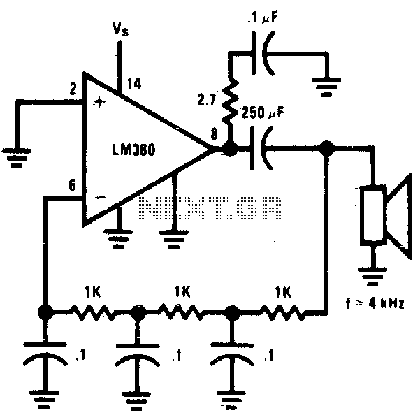
The circuit utilizes a simple RC network to generate a very high-pitched tone from a miniature speaker. With the specified component values, the circuit oscillates at a frequency of 3 kHz and drives a miniature 2W speaker at an...
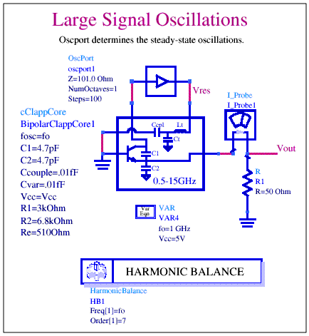
Oscillator cores (cClappCore, cHartleyCore, cModifiedClappCore, and cModifiedColpittsCore) are compatible with simulation and measurement setups outlined by the Generic Oscillator Example. These core oscillator circuits are configured for low resistance loads (50 ohms is used for these four oscillator cores,...
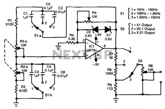
In this circuit, an LM741 operational amplifier drives a Wien-bridge network utilizing two zener diodes as an amplitude limiter. Range selection is performed by a switch that selects between capacitors (C1 through C6), while tuning is achieved using a...
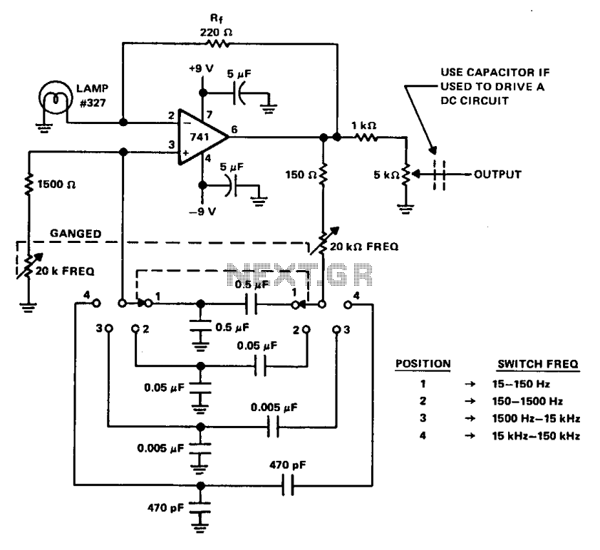
A Wien bridge oscillator generates sine waves with a very low distortion level. It produces zero phase shift at a single frequency (f = Vx t RC), which is the oscillation frequency. Stable oscillation can only occur if the...
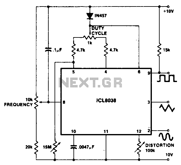
To achieve a 1000:1 sweep range, the voltage across the external resistors Ra and Rb must be reduced to nearly zero. This necessitates that the maximum voltage on control pin 8 surpasses the voltage at the top of Ra...

This circuit represents a negative resistance configuration. All previous circuits utilize RC time constants to achieve resonance. LC combinations can also be employed, providing good frequency stability, high Q factor, and rapid startup. In this circuit, a signal input...