
High Current LM317 CV Power-Supply
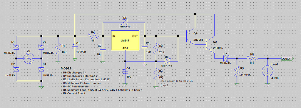
The circuit design is intended to operate within a voltage range of 0V to 24V, with a maximum current output of 4A. The inclusion of a microcontroller and an LCD display for monitoring voltage and current enhances the functionality of the circuit, allowing for real-time feedback and adjustments.
The LM317 voltage regulator serves as a critical component in this configuration. It is essential to ensure that the voltage setting resistors are selected based on reliable sources to maintain regulatory compliance and operational stability. The suggestion to implement a range limiter using series resistors with the potentiometer is prudent, as it can prevent excessive voltage or current from damaging the circuit components.
Replacing outdated components such as the 2N3055 with modern alternatives is recommended to enhance reliability and efficiency. Components like the MJ series transistors or a Darlington configuration could provide improved performance. The use of a Darlington pair can be advantageous due to its high current gain, but care must be taken to ensure that the transistor pair is appropriate for the load requirements.
The ballast load resistor specification should be re-evaluated to determine if a less precise component can be used without compromising performance. The LM317's sensing capabilities must be understood, as it may not accurately reflect the true output if the Darlington pair experiences issues. Therefore, placing resistors such as R3 and R4 at the true output is advisable to ensure accurate feedback.
The diodes in the circuit, particularly D2 and D4, must be rated adequately to handle the expected ground current. Ensuring that these diodes have ratings equivalent to D1 and D3 is crucial to prevent failure under load conditions. The configuration of D5 and D6 should also be assessed, as their current handling requirements are likely lower than those of D2 and D4.
The feedback loop involving the LM317 should be carefully considered, as it impacts the overall regulation of the output voltage. Utilizing a high-current regulator circuit from the LM317 datasheet may offer a more robust solution. The potential need for a separate sense pin to improve regulation accuracy should also be explored, particularly in high load scenarios.
Considering the input voltage, which is expected to be slightly higher than the maximum output, the thermal management of the output transistors is critical. The dissipation of 100 watts or more necessitates the use of multiple transistors to share the thermal load, ensuring that no single component is pushed beyond its limits. This approach will enhance the circuit's longevity and reliability while maintaining performance within specified operating conditions.The voltage range will be 0V to 24V and I don`t expect to use any more than 4A. A micro and LCD could probably be added to measure voltage and current. Here is the schematic: Basically the circuit looks more or less OK. Regarding the voltage setting resistors of the 317 I would check the literature, so that you don`t end up bending the rules out of shape. Also you might want to think some kind of range limiter resistors in series wiuth the pot. I am not sure if the regulator likes a short in the divider. But then again it may - can`t remember offhand. Its been a while since i played with 317s. Please throw the 2N3055s out and put in something invented during this millennium. The days of those dinosaurs is truly past. Something starting "MJ. " would be the thing to specify in my opinion. Or why not just use a Darlington in the first place. Finally, you seem to have a really exact spec for the ballast load resistor. Do you really need it to be that precise If you need a milliamp, OK but surely 1, 2 mA or whatever you would get from one E12 series component would do as well. probably. and most likely. your LM317 is sensing its output. not the "true" output. so if something whacky going on to the darlington, lm317 will not aware of it. and blimey, if the darling going whacky, its not pretty, esp when you have precious gem on the "true" output.
my bet is put the R3, R4 et al at the "true" output. D2 and D4 aren`t rated high enough. They need to be rated the same as D1 and D3. All of the current that goes to your circuit`s ground is going to go through either D2 or D4. With the current circuit configuration, D5 and D6 don`t need to be nearly as beefy. Perhaps you swapped them with D2 and D4 Right now the only current they will see is what gets discharged from C3 or C4. Finally, like Mechatrommer pointed out, the LM317 isn`t in the overall feedback loop so it isn`t truly regulating the output.
The LM317 is really just serving as a voltage reference for the base of the Darlington pair in this configuration. You might consider basing your circuit on one of the `high current` regulator circuits that can be found in the LM317 datasheet.
The comment about the feedback loop sounds right. Reason why i said nothing is that i seem to recall a paper that recommended doing it like this instead of directly from the output. There was some other reason except accuracy of regulation but i cannot remember what it was and can`t locate the paper to check.
Unless there`s a particular reason why you`ve done it, a darlington pair in this type of application would normally consist of a medium power, medium gain transistor followed by your high power, low gain model. If you did need to use a darlington pair, perhaps consider something like a BD139. Being a lower power transistor, it has a higher Hfe, smaller footprint and it`s cheaper. You don`t say what you`re input voltage is, but assuming it`s a couple of volts high than your max output, say 28V.
When you pulling 4A @ 1V from the output, you`re dissipating 100 watts or more in the output transistor. That`s just too much for one transistor, it can dissipate 115W if you keep the transistor case temp down at 25 degrees C, which is totally impractical.
I would spread it across a few of them. The comment about the feedback loop sounds right. Reason why i said nothing is that i seem to recall a paper that recommended doing it like this instead of directly from the output. There was some other reason except accuracy of regulation but i cannot remember what it was and can`t locate the paper to check.
Now that I think about it, you`re right. It`s probably because of the 1. 25V reference between OUT and ADJ. The part would need a separate sense pin to work the way I suggested. Just want to say Thank You for taking time to review my circuit and give 🔗 External reference
Related Circuits
This circuit design for a low current relay is intended for use in battery-operated electronic devices, with an operating current in microamperes (µA). It utilizes a bistable relay and additional components to enable the relay to function similarly to...
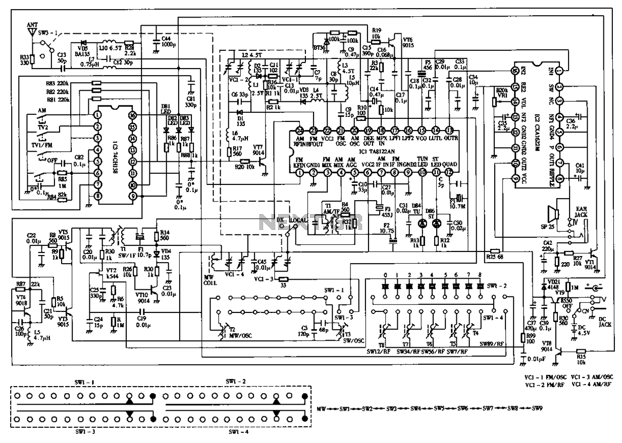
The circuit diagram for the Desheng 119 700 type FM, TV sound, medium wave, and short wave high sensitivity L2-band stereo radio is presented below. The Desheng 119 700 type radio circuit is designed to receive various frequency bands including...
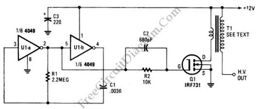
The schematic diagram below illustrates a high voltage generator circuit. This circuit employs a 4049 hex inverter functioning as an oscillator, with the option to utilize an ignition transformer from an automotive engine. A flyback transformer may also be...
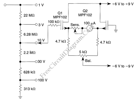
The voltmeter illustrated in the schematic diagram below possesses a very high input impedance. The range selector employs standard voltage divider resistors; however, due to the subsequent preamplifier utilizing JFETs, the divider can be designed with very high resistance...

Microsemi's LX6512 is a cost-effective, Direct Drive CCFL (Cold Cathode Fluorescent Lamp) controller. The integrated controller is optimized to drive CCFLs (Cold Cathode Fluorescent Lamps). The Microsemi LX6512 is designed to provide efficient and reliable operation for driving Cold Cathode...
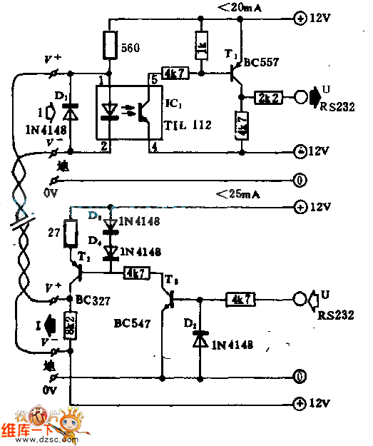
This circuitry facilitates the connection between the computer's Z RS-23 serial interface and the current ring circuitry. It converts the voltage signal of the transmission into a current signal of 20 mA, achieving a maximum speed of 1200 bits....
Warning: include(partials/cookie-banner.php): Failed to open stream: Permission denied in /var/www/html/nextgr/view-circuit.php on line 713
Warning: include(): Failed opening 'partials/cookie-banner.php' for inclusion (include_path='.:/usr/share/php') in /var/www/html/nextgr/view-circuit.php on line 713