
high gain antenna 43dB amplifier circuit
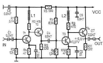
This antenna amplifier circuit is particularly advantageous for enhancing weak signals in the specified frequency range, making it suitable for various radio applications. The choice of transistors, such as the BF183 or BF200, ensures reliable performance and compatibility within the circuit. These transistors are known for their low noise characteristics, which contribute to the overall effectiveness of the amplifier.
The design includes two inductors, L1 and L2, which are essential for tuning the amplifier to the desired frequency range. The specification of using 0.25 mm CuEm wire for the coils ensures minimal resistance and optimal inductance, while the 5 mm diameter allows for a compact design. The requirement of 10 turns for each coil is a critical design parameter that determines the inductance value, which is necessary for achieving the desired gain and frequency response.
With an input and output impedance of 75 ohms, this amplifier is well-suited for integration with standard RF systems, ensuring minimal signal reflection and maximum power transfer. The low power consumption of 20 mA makes this amplifier an energy-efficient choice, allowing it to be powered by battery-operated devices or low-power supply circuits.
Overall, this antenna amplifier circuit is an excellent solution for individuals seeking to improve signal reception in the specified frequency range, combining simplicity, efficiency, and effectiveness in its design.A very simple and useful antenna amplifier can be constructed using this circuit diagram. This antenna amplifier is very useful for 35kHz-150Mhz frequency band. This antenna amplifier circuit is based on transistors and has a low 3 dB non-linearity and a high gain of 43 dB. The input and output impedance for this rf amplifier is 75 ohms. The L 1 and L2 radio frequency coils are constructed from a 0. 25 mm CuEm wire, with a 5 mm diameter. Both coils require 10 number of turns. All used transistors are of the same type and can be BF183, BF200 or other similar type. The total consumption of this rf amplifier is very low, the circuit will need only 20 mA. 🔗 External reference
Related Circuits
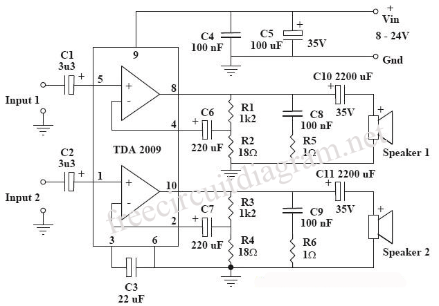
This circuit is a diagram of a mini amplifier. The amplifier circuit has a power output of 10 watts and is well-suited for car audio applications. It utilizes the TDA2009A integrated circuit as the power amplifier. To prevent excessive...
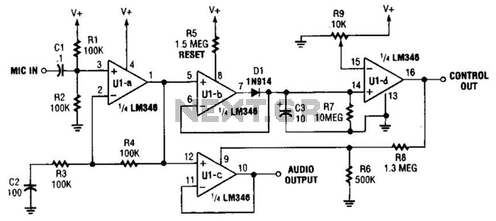
In specific applications, such as transmitters or other communications and control systems, this circuit is designed to be beneficial. It provides both audio output and DC control outputs. Additionally, R9 establishes the control threshold. The circuit in question is versatile...
This is the schematic diagram of a 300W power inverter circuit. The inverter utilizes the MJ15003 power transistor for final amplification. If the MJ15003 transistor is difficult to source, it can be replaced with a 2N3773. The inverter is...
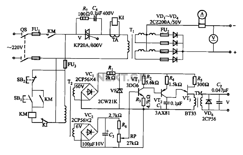
A 500A-6V single-phase power supply circuit designed for thyristor electroplating. This circuit can output a continuous DC current of 500A at 6V, which is adjustable for plating processes. It incorporates a single-junction transistor as part of the trigger circuit,...
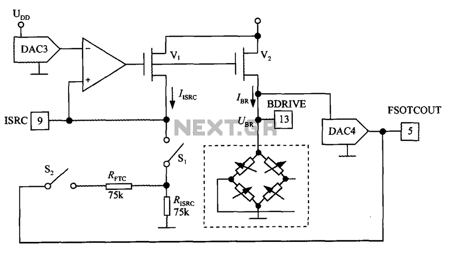
The excitation circuit for the digital pressure signal conditioner MAX1458 is illustrated. The output DAC3 is utilized to adjust the sensor excitation current (IBR), enabling full-scale fine calibration. The reference current (IISRC) is determined by the resistor RISRC and...
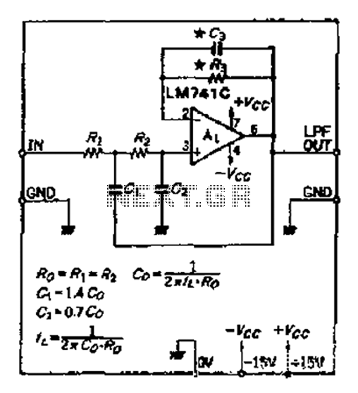
A 12dB/oct Butterworth filter circuit is designed to achieve a flat frequency response. The optimal value for the circuit's Q factor is 0.707, which ensures a flat characteristic. The feedback capacitance must be selected to maintain high capacity and...
Warning: include(partials/cookie-banner.php): Failed to open stream: Permission denied in /var/www/html/nextgr/view-circuit.php on line 713
Warning: include(): Failed opening 'partials/cookie-banner.php' for inclusion (include_path='.:/usr/share/php') in /var/www/html/nextgr/view-circuit.php on line 713