
High Input Voltage Linear Regulator
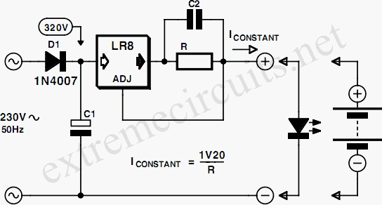
The LR8A voltage regulator is a versatile component designed for high-voltage applications, making it suitable for various electronic circuits requiring stable voltage outputs. Its ability to handle input voltages up to 450V allows it to be integrated into systems with high voltage levels, such as industrial power supplies and high-voltage LED drivers.
The adjustable output voltage feature, facilitated by resistors R1 and R2, provides flexibility in circuit design, enabling engineers to customize the output voltage according to specific requirements. The internal bias current and the feedback mechanism ensure that the output voltage remains stable despite variations in input voltage and load conditions.
For applications where temperature management is critical, the built-in thermal protection feature prevents overheating, thereby enhancing the reliability and longevity of the device. The output current limitation further protects the circuit from potential damage due to overload conditions.
The dual application capability of the LR8A as both a voltage regulator and a constant current source expands its utility, allowing it to efficiently drive LEDs across a wide voltage range. This adaptability is particularly beneficial in applications where power efficiency and thermal management are paramount.
The inclusion of diode D1 in the circuit design is a crucial safety feature, ensuring that the output does not exceed the input voltage, which could otherwise lead to circuit failure. The calculation of the minimum input capacitor C1 is essential for ensuring stable operation, particularly in rectified AC applications where voltage fluctuations can occur.
Overall, the LR8A from Supertex Inc represents a significant advancement in linear voltage regulation technology, providing engineers with a robust solution for high-voltage applications while maintaining performance and reliability.Commonly used 3-pin linear voltage regulators, for example the LM317, cannot handle input voltages in excess of about 30V. The LR8A from Supertex Inc is a new, adjustable three pin regulator that can accept input voltages up to 450V and can supply an output current of 0.
5mA to 10mA. Using this device it is possible to work with rectified 230VAC. T he LR8 has a wide input voltage range of +12 V to +450V. Two external resistors (R1 and R2) allow the output voltage to be adjusted from 1. 20 V to 440 V provided that the input voltage is at least 10 V greater than the output voltage. The LR8 adjusts the voltage difference between the Vout and ADJ pins to a nominal value of 1. 20V. This 1. 20V is amplified by the external resistor ratio of R1 and R2. An internal constant bias current of 10 µA is connected to the ADJ pin so that Vout is increased by a constant voltage of 10 µA times R2. The formula for calculating the output voltage is given next to the circuit diagram. To ensure stable operation of the regulator a minimum output current of 500 µA is necessary and a bypass capacitor of minimum 1.
0 µF should be used. Protection circuits in the LR8 limit the output current to 15mA typically and temperature protection ensures that the device temperature will not exceed 125oC. When the device reaches its temperature limit, the output voltage/current will decrease to keep the junction temperature within limits.
The two circuit diagrams show the LR8 used as a voltage regulator and as a constant current source. The current source can be used to a drive an LED. This conguration would give an LED with super-wide input voltage range, i. e. , from +12V to +450V. The LR8 was originally designed to be used for switch mode supply start-up applications so it incorporates a feature which shuts down the LR8 when the output voltage exceeds the input voltage. Diode D1 is therefore necessary in the voltage regulator circuit diagram to prevent the output voltage exceeding the input voltage at any time.
The minimum value of the input capacitor C1 can be calculated from the following formula: C1(min) = (IL t ) / (Vpk Vout 10V) Where IL is the load current, and t the period between two voltage peaks. At 50 Hz, using one rectifying diode this will give a value t = 20 ms. Vpk is the peak input voltage, while Vout is the selected output voltage. The LR8 is available in two package outlines. The LR8N8 is a SOT89 SMD package while the LR8N3 is the familiar TO92 Transistor outline (e. g. BC 238). The TO-92 package can dissipate a maximum of 0. 74W while with suitable heatsinking, the SMD package can dissipate 1. 6W. 🔗 External reference
Related Circuits
The 60-watt linear amplifier is a straightforward all-solid-state circuit utilizing the power MOSFET IRF840. The IRF series of power transistors is available in various voltage and power ratings, with a single IRF840 capable of handling a maximum power output...
Current negative feedback voltage divider biased circuit diagram. The current negative feedback voltage divider biased circuit is a configuration commonly used in electronic amplifiers to stabilize the operating point and improve linearity. This circuit typically consists of an amplifier, a...
This high voltage generator is capable of producing a stable high voltage exceeding 8kV. The circuit design is straightforward, ensuring stability and reliability. It consists of a step-down rectifier, a voltage regulator circuit, an 18kHz multivibrator-type oscillator, and a...
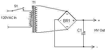
The circuit can produce about 250-500mA at 2KV, depending on the transformer. For C1, you can use the capacitor out of an old microwave. This circuit is mainly provided as a demonstration of using commonly available parts for something...
Construct a logic level shifter using discrete components such as transistors and resistors, or opt for a single-component solution with an integrated circuit (IC). Many ICs do not accept input voltages as low as 1.4 V; however, the Fairchild...

Common mode input voltage up to a difference of 100V enlarged circuit diagram. The circuit diagram described features a design capable of handling a common mode input voltage with a differential range of up to 100V. Such a configuration is...