
level shifting Increasing Voltage

To implement a logic level shifter using the Fairchild FXLP34P5X IC, the circuit design can be outlined as follows:
1. **Power Supply Connections**: The circuit requires two power supply connections. Vcc1, which is the lower voltage supply, should be connected to 1.4 V. This is the logic level for the low input signal. Vcc, which is the higher voltage supply, can be connected up to 3.6 V, providing the necessary high-level output voltage.
2. **Input Signal**: The low-level input signal should be connected to pin A of the FXLP34P5X. This pin is designed to accept signals from devices that operate at lower voltage levels.
3. **Output Signal**: The output signal is taken from pin Y, which will provide the shifted high-level output signal. This output can be interfaced with higher voltage logic circuits, ensuring compatibility between devices operating at different voltage levels.
4. **Resistors and Transistors (if using discrete components)**: If a discrete component approach is preferred, N-channel and P-channel MOSFETs can be used in combination with appropriate resistors to create a bidirectional level shifter. The resistors would be used to pull up the gate of the MOSFETs to the respective supply voltages, ensuring proper operation of the level shifting mechanism.
5. **PCB Layout Considerations**: When designing the PCB, care should be taken to minimize trace lengths between the IC and the signal connections to avoid signal integrity issues. Additionally, proper decoupling capacitors should be placed close to the power pins of the IC to filter out noise and stabilize the power supply.
6. **Testing**: After constructing the circuit, it is essential to test the functionality by applying low-level input signals and measuring the output signals to verify that the level shifting is occurring correctly.
This logic level shifter design facilitates communication between devices operating at different voltage levels, enhancing interoperability in mixed-voltage environments.Build a logic level shifter (that`s what it`s called) with a few discrete components (transistors and resistors) or you can go for a one-component solution, i. e. an IC. Most ICs won`t accept input voltages as low as 1. 4 V, but I found Fairchild`s FXLP34 which does. (You want the FXLP34P5X, the other versions have leadless packages and are therefore more difficult to solder) A is where you supply the low-level input signal, Y is your "high"-level output signal. Vcc1 is your 1. 4 V connection, connect the required output voltage to Vcc (up to 3. 6 V). 🔗 External reference
Related Circuits
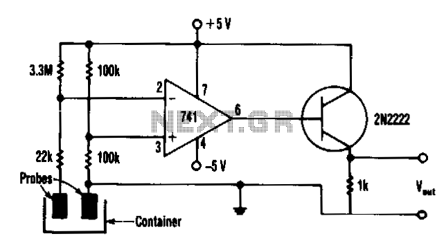
This monitor utilizes a common 741 op-amp configured as a comparator along with a low-cost non-transistor output driver. In the absence of liquid, a voltage of approximately 2.92 V is present at the inverting input (pin 2) of the...
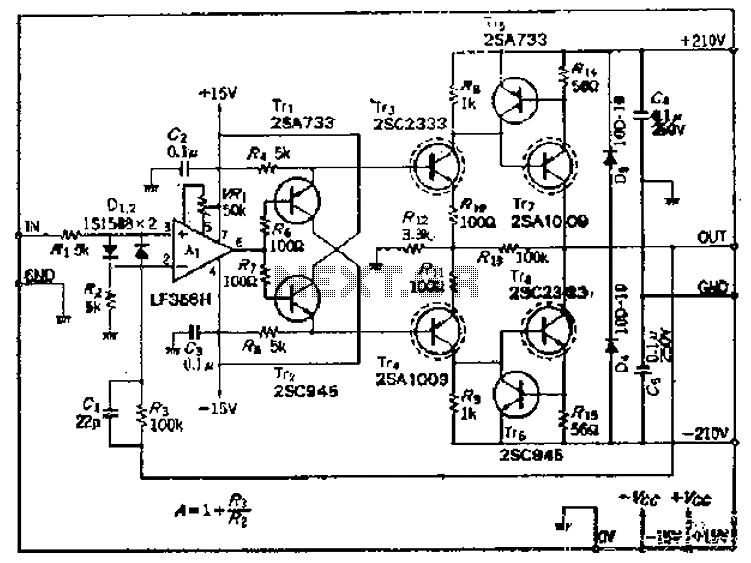
This amplifier circuit operates with an OP amplifier that is power-driven, which leads to the presence of floating voltage errors and necessitates a high-pressure booster for transistor protection. The circuit utilizes a mutual feedback configuration, connecting to the output...
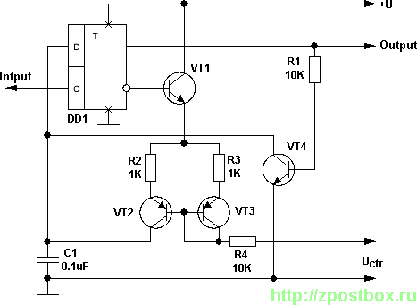
This voltage-controlled frequency divider circuit produces lower frequency pulses that depend on the control voltage, with synchronous rising edges for the input and output pulses. Typically, such frequency dividers utilize a monostable circuit connected between an inverted output and...
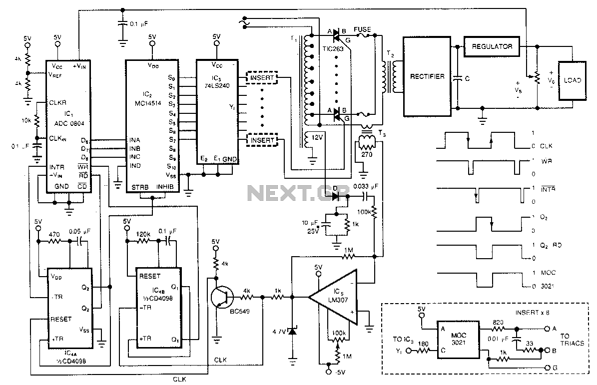
One of the control circuit's triacs selects the tap on the main transformer T1, which provides the proper preregulated voltage to the secondary regulator. T2 and its associated components comprise the secondary regulator. The ADC 0804, IC1, digitizes a...
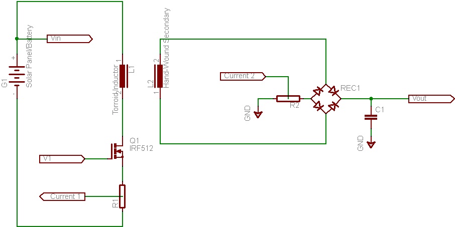
This document discusses the future direction of the Free Charge Controller project and proposes a new solar charge controller circuit. The Free Charge Controller project aims to enhance the efficiency and effectiveness of solar energy management systems. The proposed solar...
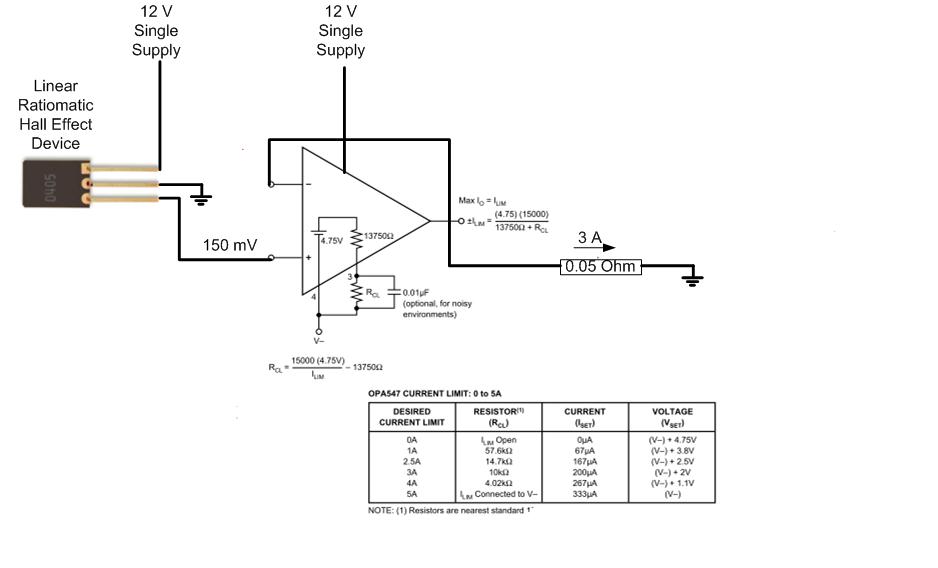
The proposed approach would dissipate (12V)(3A) = 36 watts, which results in significant heat generation in the circuit. This necessitates consideration of two alternatives: 1) Operating the op-amp at a lower supply voltage, if feasible, or 2) Utilizing a...