
High power mobile phone Jammer circuit

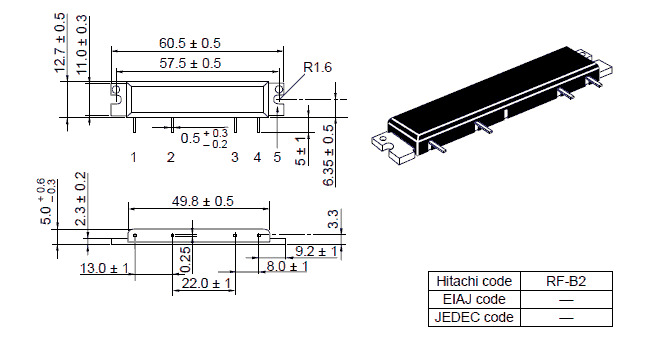
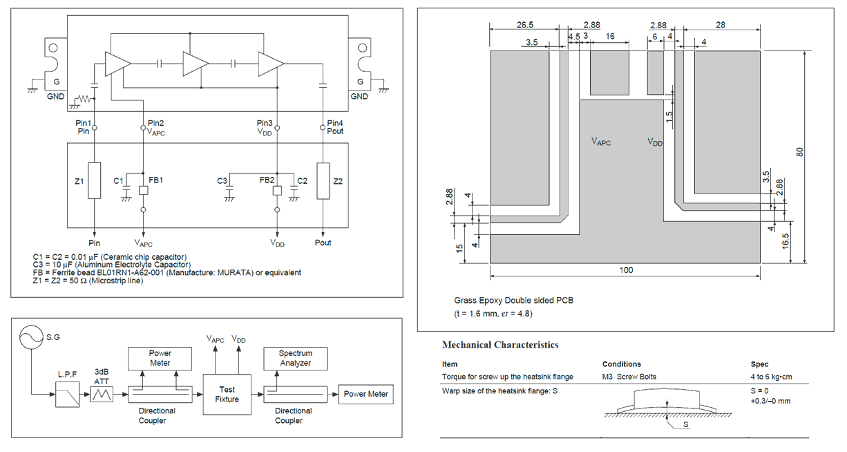
The jammer's output focuses on the PF0030 MOSFET amplifier by Hitachi, which offers high stability with a voltage standing wave ratio (VSWR) of 20:1 and a low control current of 400 mA. Key considerations for the PF0030 include ensuring minimal unevenness and distortion on the heat sink surface (less than 0.05 mm) and avoiding dust between the module and heat sink. The module should be mounted no more than 1.5 mm from the PCB, with soldering temperatures and times limited to 230°C for 10 seconds. Thermal joint compound type G746 from Shin-Etsu Chemical, Co., Ltd. is recommended. Precautions against electrostatic damage should be taken, including grounding soldering irons and measuring equipment. The torque for securing the heat sink flange should be between 4 to 6 kg·cm using M3 screws. The module should be secured before soldering leads, and mechanical and thermal stresses should be avoided. Changes to external components should be evaluated for their impact on electrical characteristics. The module should not be washed, except for lead pins, and the ground impedance between the module's GND flange and PCB GND should be minimized.
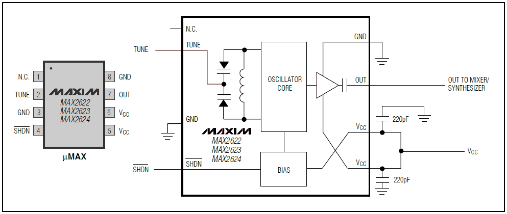
The circuit utilizes the MAX2622, a self-contained voltage-controlled oscillator (VCO) that integrates an oscillator and output buffer in a miniature 8-pin MAX package. The VCO's tank circuit components are integrated on-chip, simplifying its application. The center frequency and frequency span are factory preset, with an external tuning voltage controlling the oscillation frequency. The output signals are buffered by an amplifier matched to 50 ohms. The MAX2622 employs an LC oscillator topology, with the tuning input connected to the output of a phase-locked loop (PLL) loop filter, which should provide a low-impedance source. To minimize FM noise, a simple RC filter may be used during testing.
Proper layout techniques are essential for high-frequency signals, including the use of controlled impedance lines and placing decoupling capacitors close to VCC pins. A low-inductance path to ground should be ensured, with GND vias positioned near the device. The circuit emits a carrier that sweeps across the cellular band.
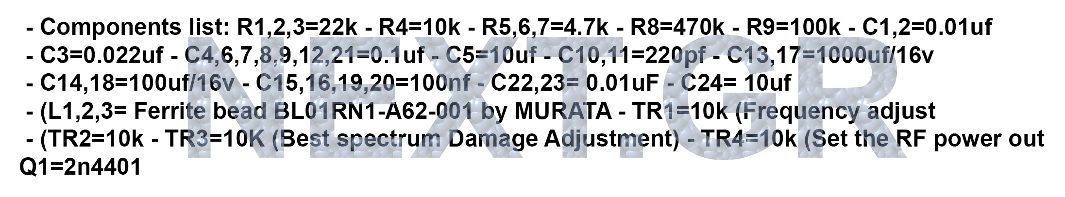
The S-80830ALY regulator by SEIKO is a high-precision 3V device, and other similar regulators may be used. The 78L05 provides 5V to a ~1 kHz sweeper circuit, which consists of an NPN transistor (2N4401) and an LM741 operational amplifier, along with the MAX2622 for oscillation. TR1 serves as the main frequency adjuster, while TR3 adjusts the signal for optimal spectrum interference, set to slightly less than 1V peak-to-peak. TR2 tunes the output to approximately 880 MHz (~1.2V), while TR4 adjusts the RF power output to 200-300 mW. Grounding the PF0030 MOSFET amplifier and using an appropriate heatsink is crucial. Coaxial cable RG58 or other 50-ohm types should connect the MAX2622's pin 7 to the PF0030's pin 1, with RF levels not exceeding +13 dBm. A high-gain omnidirectional antenna is recommended for best results. This circuit may also interfere with 800 MHz radios and SMR radios, potentially affecting devices operating in the 2.4 GHz ISM band. Caution is advised when operating this device.** UPDATED 2014 ** This project is the original High power mobile phone Jammer circuit, and all updates are posted here. All other versions are just copied from next.gr. First off all you should be very careful how to use this device. Its fully illegal and so the purpose I post this Circuit is only for educational and testing reasons.
This type of device is being used by security for VIPS, specially at their limousines to avoid bomb triggering while the car passes from the target cell phone-bomb. Offcourse there are those who use it to make a joke or to make the people crazy in the square block you are.
The power of the jammer is already enough to do your thing, but certainly you can place a 30W linear power amp at the RF output and block a much wider area. So next.gr advice you, Be nice person with that and remember that there are people who may need desperately to receive or make a call and one of them could be you!
And if you can't resist of operating the jammer do it for few secs. Do not forget that if you connect linear amp the unit will be a current sucker after all.
** UPDATED 2014 **
The Jammer output focus around PF0030 MOSFET amplifier by Hitachi, which offers high stability of VSWR = 20 : 1 and low power control current of 400 mA. Few things about PF0030: · Unevenness and distortion at the surface of the heat sink attached module should be less than 0.05 mm.
It should not be existed any dust between module and heat sink.
· MODULE should be separated from PCB less than 1.5 mm. · Soldering temperature and soldering time should be less than 230°C, 10 sec. (Soldering position spaced from the root point of the lead frame: 2 mm) · Recommendation of thermal joint compounds is TYPE G746. (Manufacturer: Shin-Etsu Chemical, Co., Ltd.) next.gr· To protect devices from electro-static damage, soldering iron, measuring-equipment and human body etc.
should be grounded. · Torque for screw up the heatsink flange should be 4 to 6 kg · cm with M3 screw bolts. · Don’t solder the flange directly. · It should make the lead frame as straight as possible. ·
The module should be screwed up before lead soldering. · It should not be given mechanical and thermal stress to lead and flange of the module. · When the external parts (Isolator, Duplexer, etc.) of the module are changed, the electrical characteristics should be evaluated enough.
· Don’t washing the module except lead pins. · To get good stability, ground impedance between the module GND flange and PCB GND pattern should be designed as low as possible. Next.gr comes the MAX2622 a self-contained voltage- controlled oscillators (VCOs) combine an integrated oscillator and output buffer in a miniature 8-pin ?MAX package.
The inductor and varactor elements of the tank circuits are integrated on-chip, greatly simplifying application of the part.
In addition, the center frequency of oscillation and frequency span are factory preset to provide a guaranteed frequency range versus control voltage. An external tuning voltage controls the oscillation frequency. The output signals are buffered by an amplifier stage matched on-chip to 50?.
The MAX2622 VCO is implemented as an LC oscillator topology, integrating all of the tank components on-chip.
This fully monolithic approach provides an extremely easy-to-use VCO, equivalent to a VCO module. The frequency is controlled by a voltage applied to the TUNE pin, which is internally connected to the varactor. The VCO core uses a differential topology to provide a stable frequency versus supply voltage and improve the immunity to load variations.
In addition, there is a buffer amplifier following the oscillator core to provide added isolation from load variations and to boost the output power. Output Buffer:The oscillator signal from the core drives an output buffer amplifier. The amplifier is constructed as a common-emitter stage with an integrated on-chip reactive output match.
No external DC blocking capacitor is required, eliminating the need for any external components. The output amplifier has its own VCC and GND pins to minimize load-pulling effects. The amplifier boosts the oscillator signal to a level suitable for driving most RF mixers. Tune Input: The tuning input is typically connected to the output of the PLL loop filter. The loop filter is presumed to provide an appropriately low-impedance source. It may incorporate an extra RC filter stage to reduce high-frequency noise and spurious signals. next.gr. Any excess noise on the tuning input is directly translated into FM noise, which can degrade the phase-noise performance of the oscillator. Therefore, it is important to minimize the noise introduced on the tuning input.
A simple RC filter with low corner frequency is needed during testing in order to filter the noise present on the voltage source driving the tuning line.
Layout Issues: Always use controlled impedance lines (microstrip, coplanar waveguide, etc.) for high-frequency signals. Always place decoupling capacitors as close to the VCC pins as possible; for long VCC lines, it may be necessary to add additional decoupling capacitors located further from the device.
Always provide a low-inductance path to ground, and keep GND vias as close to the device as possible. Thermal reliefs on GND pads are not recommended. Circuit Description: The circuit emits a carrier that sweeps across the cellular band.
The Regulator S-80830ALY is made by SEIKO and is a 3V high precision device and you can use any other similar regulator.
The 78L05 on the other hand provide with 5 volts the ~1KHz sweeper circuit (which consist from the NPN transistor 2N4401 and the LM741) and the MAX2622 who does the oscillation to the desired frequency. TR1 is the main frequency adjuster and TR3 adjust the signal for best spectrum damage and should be set to slightly less than 1 Volt peak to peak.
TR2 is for tunning the output of approximately 880 MHz (~1.2V). You can use any 12V power supply and 1A should be enough. Finally TR4 adjusts the RF power output to 200-300 mW. Do not forget to ground the PF0030 MOSFET amplifier and put a nice heatsink as well. Coaxial cable RG58 or any other type 50hom cable should be used between the pin7 of MAX2622 and pin1 of Hitachi PF0030 (RF to that point should be +13dBm MAX) and offcourse coaxial at the output to the antenna. Coils L1, L2 and L3 are Ferrite Beads. For antenna, if you want best results, you need a high gain omnidirectional antenna. Can also be used to jam 800 MHz radios as well as SMR radios and may do damage to ISM 900 MHz band. The third harmonic of a sweeping 800 - 828 MHz signal will jam devices operating in the 2.4 GHz ISM band.
Anyway by careful with that little monster.
Related Circuits
Here is a simple transmitter that when connected to a phone line, will transmit anything on that line (except the dial tone) to any FM radio. The frequency can be tuned from 88 to about 94 MHz and the...
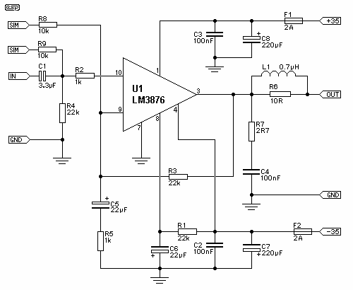
The supply voltage should be about +/- 35 Volts at full load, which will let this little guy provide a maximum of 56 Watts (rated minimum output at 25 degrees C). To enable maximum power, it is important to...
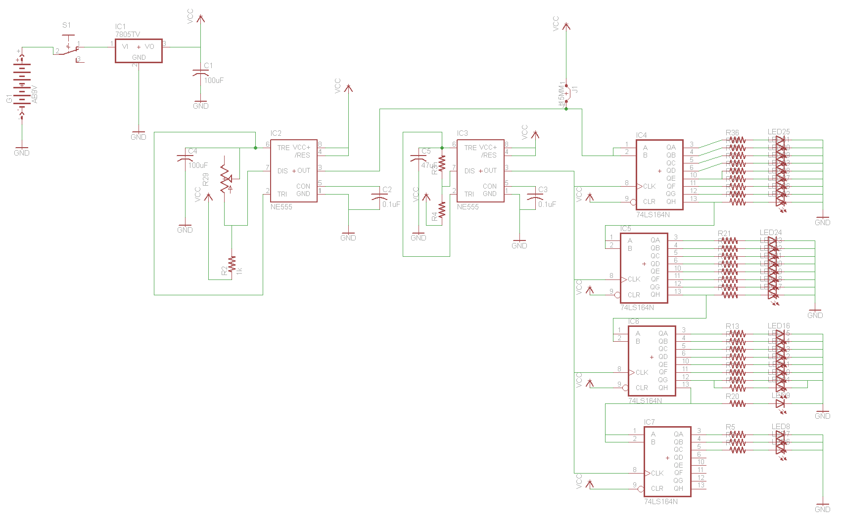
For the two-layer board schematic, six core integrated circuits (ICs) will be utilized: four 74LS164 shift registers and two 555 timers. The schematic will be constructed using the Eagle Layout Editor, as all required components are available in its...
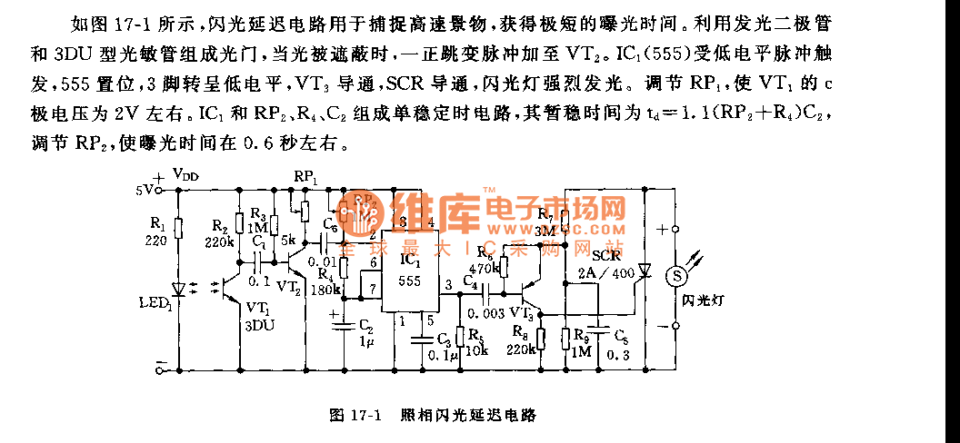
As shown in figure 17-1, the camera flash delay circuit is designed to capture high-speed scenes, allowing for very short exposure times. The light gate consists of a luminous diode and a 3DU type photosensitive tube. When the light...
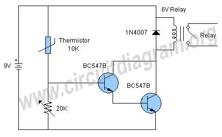
The circuit operates based on a desired temperature setting. It can be utilized for various applications, such as turning on a fan at a specified temperature or activating an emergency temperature alarm. The power supply for the circuit can...
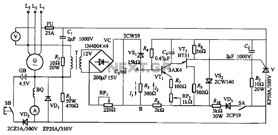
The circuit depicted in Figure 7-32 is designed for an excitation device capable of handling a terminal voltage of 400V and a capacity of less than 75kW for synchronous generator motors, enabling automatic adjustment of excitation. When the generator...