
High quality FM transmitter
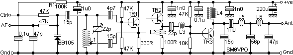
TR2 (BC547) is both biased and directly connected to the Emitter of TR1, which is a little unconventional in a VHF circuit. I needed to get a good input to TR2 and cut down on components. There are already far too many coils as it is in this circuit. Remember that the BC547 is an audio transistor but works well at VHF. The inductor in the Emitter of TR2 helps to extend the response a little to give a bit more signal to drive the final power amplifier transistor (TR3). TR2 gives no voltage gain; it is current we need to drive TR3. We already have enough volts from the oscillator.
22pf and L3 couple TR2 output into the Base of TR3. These components match the impedances so we get the maximum power possible into TR3 Base. The signal level, however is still quite low, so some DC biasing has been added to turn TR3 ON a bit. The transistor should draw about 5mA with no signal. This is not enough to make it become linear, but it is operating around class "B". This would make a very poor frequency multiplier, so harmonics are also reduced a little by the DC bias. Note that NO emitter resistor has been used. The prototype units all worked well without one and the drive level is not enough to cause the transistor to conduct very much. The small standing DC bias of 5mA doesn’t even "tickle" TR3. In operation the DC voltage on the Base of TR1 will be negative due to the drive level, conduction of TR3 Base/Emitter junction and the 22pf capacitor. TR3 does NOT need a heatsink.
If you want to use a different transistor in place of TR3 then it is suggested to remove L3 and substitute a current meter in place of L4. Apply volts to the transmitter. The current should be about 5mA. Select the value of the 47K resistor if required. Any current reading between about 2mA to 8mA will suffice.
The collector of TR3 (2N4427) has a large choke to pass the supply DC, but presents a high impedance to RF. The RF signal is then matched to 50 Ohms with the 15p, L5, and 56p. The 1nF capacitor simply blocks the supply voltage that would otherwise pass to the antenna. L5 and 56p form a low-pass filter that helps to block harmonics present in the output signal. L6 and 47p are added to further reduce the harmonic levels. This filter is essential for all transmitters to avoid interference with other radio users. L5 and L6 have been positioned on the PCB to allow some coupling between them, which cancels out any residual signals outside the filter's passband. This design consideration has significantly improved the cleanliness of the prototype, achieving harmonic levels reduced to -60dBc at all supply voltages. With an output of 150mW, this corresponds to a 3rd harmonic level of 150 nano-watts and a 2nd harmonic level of just 50 nano-watts.
Adjustments to the coil values can yield an additional 2 to 3dB of output. The design intentionally mis-tunes certain components to enhance impedance matching and resonance at the band edges. The performance remains stable across the frequency range. The oscillator's frequency is influenced by L1 and the tuning capacitors, and care has been taken to avoid traditional coil winding to prevent microphony effects. The PCB design incorporates a coil etched onto the board to mitigate microphony and temperature-induced frequency variations. L2, wound on small ferrite beads, is placed in series with the emitter of TR2 to maintain stability and prevent radiation like a loop antenna. It consists of 4 turns of 0.15mm diameter enamelled wire, ensuring effective performance without unnecessary complexity.This will probably be one of the last transmitters for the 88MHz to 108MHz band. This particular TX is of special interest to those wishing to build low power Power Amplifiers for the VHF bands since it used impedance matching, power amplifier and antenna filtering, all of which should be used by radio constructors, whether it be for amateur radio or any other form of radio. The features of this project are: Higher output power - 150mW min (at 9v) and 300mW+ (at 12.5v). Very pure output signal due to carefull design and filtering. VARICAP modulation - possiblity to add a synthesiser. Single sided Printed Circuit Board, only 40mm x 72mm. Covers the domestic FM band - 88MHz to 108MHz. Easy to build, but coil winding experience IS required. The circuit itself is fairly conventional, with a couple of small refinements. It all begins with TR1 (BC547) in an inverted Hartley oscillator configuration. The feedback to the Base of TR1 is via a small 4.7pf capacitor to help keep the oscillations as weak as possible whilst allowing the oscillator to be a reliable starter. The frequency of the oscillator is determined by L1 and the 22pf trimmer capacitor and functions in the range of about 76MHz to 119MHz using the PCB I have made.
The 15pf capacitor couples the top of L1 to the varicap diode which serves to add more capacitance to the tuned circuit to alter the frequency. R1 adds the supply voltage to the varicap, with a little noise decoupling (the 0.1uf capacitor). If you are to use synthesiser control then it is important to remove R1 from the circuit, then connect the synthesiser loop filter output to the terminal marked "Ctrl".
Audio is coupled to the BB105 via a 47K resistor. There is only 47pf of decoupling in order not to restrict the AF bandwidth of the complete transmitter. The AF bandwidth is flat from 3Hz to about 72KHz, but if we look beyond these limits, there is an increase of +6dB at DC.
This is because the two 47K resistors divide the AF input voltage by 2, but at DC the 0.1uf capacitor has time to charge, the two 47K resistors do not therefore divide. TR2 (BC547) is both biassed and directly connected to the Emitter of TR1, which is a little unconventional in a VHF circuit.
I needed to get a good input to TR2 and cut down on components. There are already far too many coils as it is in this circuit. Remember that the BC547 is an audio transistor but works well at VHF. The inductor in the Emitter of TR2 helps to extend the response a little to give a bit more signal to drive the final power amplifier transistor (TR3). TR2 gives no voltage gain; it is current we need to drive TR3. We already have enough volts from the oscillator. 22pf and L3 couple TR2 output into the Base of TR3. These components match the impedances so we get the maximum power possible into TR3 Base. The signal level, however is still quite low, so some DC biasing has been added to turn TR3 ON a bit.
The transistor should draw about 5mA with no signal. This is not enough to make it become linear, but it is operating around class "B". This would make a very poor frequency multiplier, so harmonics are also reduced a little by the DC bias. Note that NO emitter resistor has been used. The prototype units all worked well without one and the drive level is not enough to cause the transistor to conduct very much.
The small standing DC bias of 5mA doesn?t even "tickle" TR3. In operation the DC voltage on the Base of TR1 will be negative due to the drive level, conduction of TR3 Base/Emitter junction and the 22pf capacitor. TR3 does NOT need a heatsink. If you want to use a different transistor in place of TR3 then I suggest you remove L3 and substitute a current meter in place of L4.
Apply volts to the transmitter. The current should be about 5mA. Select the value of the 47K resistor if required. Any current reading between about 2mA to 8mA "will do nicely sir" (even without your American Express card!) The collector of TR3 (2N4427) has a big (by QRP standards) choke to pass the supply DC, but presents a high impedance to RF. The RF signal is then matched to 50-Ohms with the 15p, L5 and 56p. The 1nf cap simply blocks the supply voltage that would otherwise pass to the antenna. L5 and 56pf form a low-pass filter that helps to block harmonics present in the output signal. L6 and 47pf are added to further reduce the harmonic levels. This filter is an absolute MUST for all transmitters if one does not wish to offend every other user of the radio spectrum.
L5 and L6 have also been positioned on the PCB so that there is a little coupling between them. This coupling serves to cancel out any residual signals, not within the passband of the filter, that may be present at the input to L5. It is this effect that was responsible for the unexpected cleanliness of the first prototype, and a little layout experimenting has now reduced the 2nd and 3rd harmonics to -60dBc at all supply voltages.
With 150mW output, this corresponds to 3rd harmonic of 150 nano-watts and a 2nd harmonic level of just 50 nano-watts. I have "played around" with the values and taken a few liberties. If you want to try adjusting the coils then then will be able to get another 2 to 3dB out of the TX. I have deliberately mis-tuned a couple of times in order that impedances and resonances will improve at the edges of the band.
The result is that the performance of the transmitter does NOT vary (much) no-matter which end of the band you are operating at. As you will apreciate, L1 and the tuning capacitors all affect the frequency of the complete transmitter.
Winding L1 has therefore NOT been considered. This would result in a spring-like affair that would cause instability, or more precisely, "microphony". This is an effect where the coil wobbles about with very small mechanical movements. In severe cases you can even talk to the the circuit, as any owner of a Marconi TF995 signal generator will testify.
By using a coil etched on the PCB you will find that microphony has been eliminated. So has coil expansion with temperature. It must be remembered, however, that this circuit is STILL based upon an LC circuit and therefore subject to changes of frequency with changes of supply voltage and "hand capacitance", etc. I will cover the supply voltage changes shortly. L2 is wound on small ferrite beads. L2 is placed in series with the emitter of the buffer transistor, TR2. In the interests of stability it is very important that this coil does NOT radiate like a loop antenna.
It is composed of 4 turns of 0.15mm Dia. enamelled wire (magnet wire in the US). The grade of ferrite is unimportant, as long as it is a grey one. One complete turn is formed when the wire passes through the hole in the middle once. The ferrite is mounted vertically in the same manner as a resistor. 🔗 External reference
Related Circuits
The objective is to capture various stages of a rapid process, especially in comparison to the resolution of the human eye. Due to the lack of advanced equipment such as a high-speed film camera, a practical setup utilizing a...
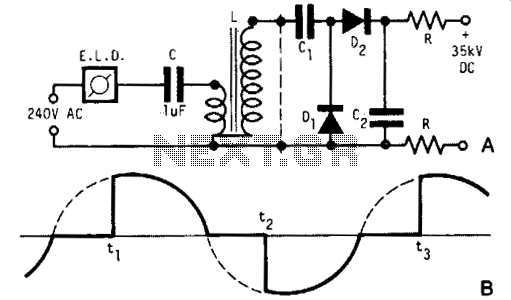
A light dimmer, a 1 µF capacitor, and a 12 V car ignition coil form a simple line-powered high-voltage generator. The current in the dimmer is illustrated in Fig. B. During the time intervals tp to t2, determined by...

AVR has two different programming modes called Parallel Programming Mode (Parallel Mode) and Serial Downloading Mode (ISP mode). In Parallel Mode, the programming is done using multiple data lines simultaneously, allowing for faster programming speeds. This mode is typically...
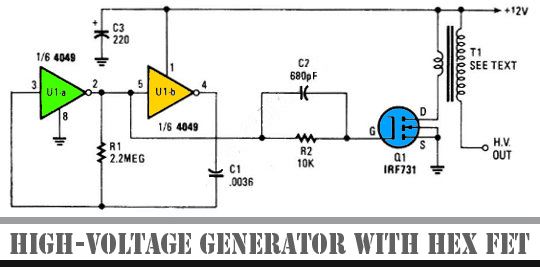
The schematic diagram below illustrates a high voltage generator circuit. This circuit employs a 4049 hex inverter configured as an oscillator, and it can utilize an ignition transformer from an automotive engine. A fly-back transformer may also be suitable....
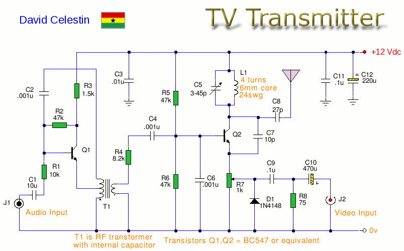
This is an analog TV transmitter. Sound modulation is of the FM type with a 5.5 MHz carrier frequency, and video transmission follows the PAL standard. The frequency can be adjusted using capacitor C5, allowing tuning from 54 to...

A tone control circuit is an electronic circuit designed to manipulate the tone of an audio signal. The tone of an audio signal is analogous to color in light. The tone control circuit typically consists of various components such as...
Warning: include(partials/cookie-banner.php): Failed to open stream: Permission denied in /var/www/html/nextgr/view-circuit.php on line 713
Warning: include(): Failed opening 'partials/cookie-banner.php' for inclusion (include_path='.:/usr/share/php') in /var/www/html/nextgr/view-circuit.php on line 713