
High Side Current Monitor
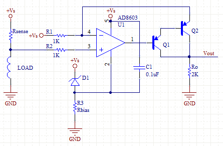
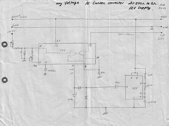
The described circuit for monitoring current on inductive loads effectively addresses the challenges associated with high-side current sensing. By employing a current sensing resistor, the design minimizes the need for more complex and costly components like current transformers or Hall effect sensors. The output voltage is shifted to a ground-referenced level, which simplifies the measurement process and enhances compatibility with standard measurement equipment.
In this circuit, the operational amplifier is configured to amplify the voltage drop across the current sensing resistor. The Zener diode D1 plays a crucial role in maintaining the operational amplifier's floating reference, allowing it to operate effectively despite the positive voltage rail. This configuration ensures that the output remains within the operational limits of the circuit, providing accurate current measurements without introducing significant errors due to ground potential shifts.
Transistors Q1 and Q2 form a feedback loop that stabilizes the output voltage. Their configuration ensures that variations in load current do not adversely affect the accuracy of the current sensing. The feedback mechanism allows for real-time adjustments to the output voltage, ensuring that it reflects the actual current flowing through the load.
The bias resistor is an essential component that ensures the operational amplifier receives adequate current for proper operation. It is critical to select a bias resistor value that balances the need for sufficient bias current while minimizing power dissipation and potential interference with the circuit's performance.
Overall, this circuit design provides a robust and cost-effective solution for monitoring current in inductive loads, making it suitable for various applications in electronics and power management systems.Monitoring current on inductive loads is a common task. It`s easier to do on the low side of a driving circuit, because a simple resistor can be used with an op-amp on the ground rail. The high side often demands that an expensive current sensing transformer or Hall effect sensor be used.
The circuit below is desirable because it uses a simple current sensing resistor instead of an transformer, and then shifts the output voltage to a ground referenced value. The zener circuit allows the op-amp circuit to float under the positive voltage rail by an amount equal to the zener voltage of D1. Transistors Q1 and Q2 are part of the feedback loop, and drive the ground referenced output resistor.
The bias resistor should allow enough current to flow for the opamp circuit. Do you need help with an electronics design Daycounter provides contract electronics design services. Contact us to give you a quote on your electronics design project. 🔗 External reference
Related Circuits
IC1 is a dual operational amplifier. In this circuit, each op-amp functions as a voltage comparator. When the voltage at the positive input exceeds the voltage at the negative input, the output transitions to a high state. Conversely, when...
The commutator circuit delivers low impedance gate drive to the PN4091 analog switch for both on and off drive conditions. This circuit also achieves near-ideal gate drive conditions for high-frequency signal handling by offering low AC impedance during off...
This circuit is capable of generating up to 1 W of audio power to drive a speaker or horn. When the CDS cell is exposed to light, its resistance decreases, activating NOR gate (a). This activation causes gates (a)...
This circuit converts a voltage control output from a process controller into a current control signal, suitable for applications such as AC drives or valves requiring a current control signal. It operates as a three-wire voltage-to-current loop converter. The...
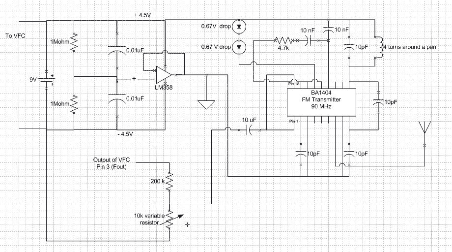
V_logic is connected to the power supply Vs and all ground are connected to the negative terminal of the battery. Fout is a square wave of varying frequency with a maximum amplitude of Vs. A voltage divider is needed...
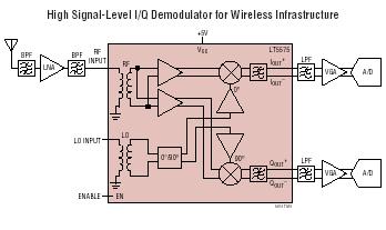
The LT5575 is an 800MHz to 2.7GHz direct conversion quadrature demodulator optimized for high linearity receiver applications. It is suitable for communications receivers where an RF signal is directly converted into I and Q baseband signals with a bandwidth...