
High-Voltage Capacitor Charger
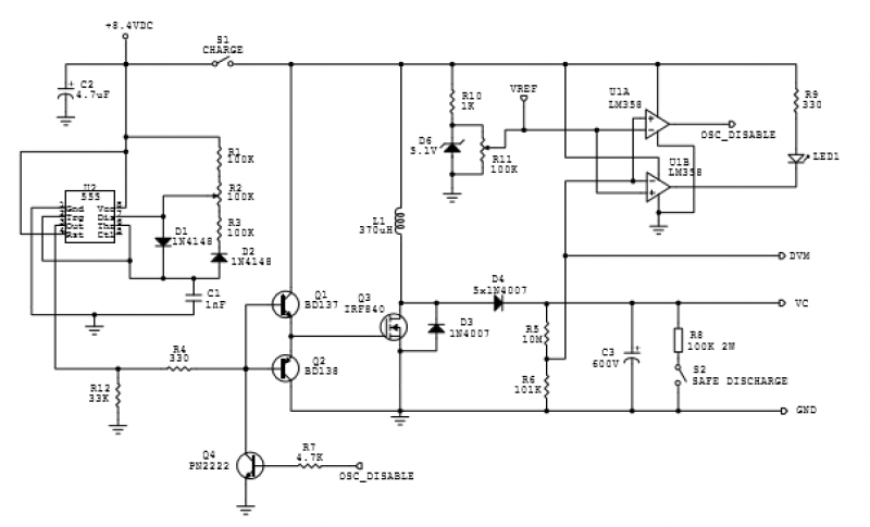
The circuit in Fig. 1 has been modified by removing R2, leading to the new configuration shown in Fig. 2. In this version, the output of the 555 timer is ON for 130µs and OFF for 80µs, resulting in a total period of 210µs and a frequency of 4762Hz. This circuit is capable of charging a capacitor up to approximately 600 VDC, suitable for high-voltage discharge experiments.
The circuit operates as a high-voltage capacitor charger, leveraging the characteristics of the IRF840 MOSFET to manage high voltage levels safely. The MOSFET’s avalanche capability is crucial for protecting the circuit from excessive voltage spikes that may occur during operation. The reference voltage (VREF) plays a significant role in regulating the output voltage across the capacitor, ensuring that it does not exceed safe limits while allowing for adjustable charging levels via the resistive divider network. The design of the inductor (L1) is critical, as its inductance value directly affects the energy transfer efficiency and the speed at which the capacitor charges. The use of a 555 timer in the modified circuit provides precise control over the duty cycle, which is essential for optimizing the charging process and maintaining the desired frequency for effective operation. Overall, this circuit exemplifies a practical application of MOSFET technology in high-voltage systems, suitable for experimental and educational purposes in electronic engineering.The circuit described here uses an IRF840 MOSFET which is rated at a maximum DSV value of 500V. The avalanche voltage is calculated as 36501. max DSA VV V. This means that up to about 600V of inductive kickback voltage may develop in the switched coil. More than that will cause the avalanche effect and turn the MOSFET ON. The circuit is shown in Fig. 1. Reference voltage (VREF) is used to set the final voltage across the capacitor by R11.
For example, a 4.27V reference indicates a charging voltage of 427V since the capacitor voltage is sensed by a 100:1 resistive divider network. If the collector of Q4 is detached from the gates of Q1 and Q2, a maximum charging voltage of about 600V is achieved.
For the circuit in Fig. 1, R2 adjusts the duty cycle. C3 is composed of two photoflash capacitors (160µF/330V) in series, making C3 an 80µF/660V capacitor. It’s observed that the capacitor is charged faster when the duty cycle is higher. L1 is a handwound inductor around a ferrite core using three layers of 0.5mm magnet wire. Measured inductance of L1 is about 370µH.
The circuit in Fig. 1 has been improved by eliminating R2 and the new circuit is shown in Fig. 2. For this one, 555 output is ON for 130µs and OFF for 80µs. Thus the period and frequency are 210µs and 4762Hz, respectively.
This circuit can be used to charge a capacitor up to about 600 VDC for HV discharge experiments.
By 4beowulf7 - [email protected]
Related Circuits
When a discharged gel cell is connected, the charger goes into a fast charge mode at a fixed rate of 400 ma. After the chip detects the voltage leveling off or when 4 1/2 hours has elapsed (whichever happens...
Using this circuit will give good charging results to a sealed lead acid battery, like I use in the metal detector. This circuit is extremely small in size and has a low parts count, making it ideal in some...

Charger for all battery types power supply. This lithium battery charger circuit is dedicated to charging lithium batteries. It uses two chips: the voltage regulator LM317T and ICL7665, which warns microprocessors of overvoltage and undervoltage conditions. Charging is completed...
After experiencing failures with four Apple iPad chargers and not wishing to incur further expenses by purchasing replacements from Apple, a decision was made to create 12V powered chargers. This would utilize the surplus photovoltaic (PV) power available during...
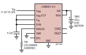
A simple and efficient lithium battery charger and monitoring system can be designed using the LTM8061 integrated circuit from Linear Technology. The LTM8061 is a high-efficiency 32V, 2A module standalone lithium battery charger optimized for one- and two-cell packs,...

This is a simple yet effective charger for lead-acid batteries. It utilizes a 12-volt car bulb as both a current regulator and a charge status indicator. The described circuit is an innovative approach to charging lead-acid batteries. It employs...