
High-Voltage Regulator With Short Circuit Protection
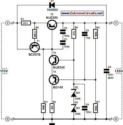
This circuit design is a robust solution for high voltage regulation, effectively managing the challenges associated with higher supply voltages. The use of a PNP transistor (T2) as the main regulating element ensures a low voltage drop, enhancing efficiency. The integration of a current limiting feature using T1 provides an essential safeguard against overcurrent situations, which is critical in maintaining circuit integrity and protecting components. The careful selection of resistor values in the potential divider (R6/R7) allows for precise voltage regulation, while the series connection of capacitors (C1 and C2) contributes to stability during transient conditions. The inclusion of zener diodes for reference voltage ensures consistent operation under varying load conditions. Overall, this design emphasizes reliability and simplicity, making it suitable for applications requiring stable high voltage regulation.There are many circuits for low voltage regulators. For higher voltages, such as supplies for valve circuits, the situation is different. That`s why we decided to design this simple regulator that can cope with these voltages. This circuit is obviously well suited for use in combination with the quad power supply for the hybrid amp, published else where in this issue. The actual regulator consists of just three transistors. A fourth has been added for the current limiting function. The circuit is a positive series regulator, using a pnp transistor (T2) to keep the voltage drop as low as possible. The operation of the circuit is very straightforward. When the output voltage drops, T4 pulls the emitter of T3 lower. This drives T2 harder, which causes the output voltage to rise again. R4 restricts the base current of T2. C1 and C2 have been added to improve the stability of the circuit. These are connected in series so that the voltage across each capacitor at switch-on or during a short circuit doesn`t become too large.
You should use capacitors rated for at least 100 V for C1-C3. D1 protects T2 against negative voltages that may occur when the input is short-circuited or when large capacitors are connected to the output. We use two zener diodes of 39 V connected in series for the reference voltage, giving 78 V to the base of T3.
Because R6 is equal to R7 the output voltage will be twice as large, which is about 155 V. T4 acts as a buffer for potential divider R6/R7, which means we can use higher values for these resistors and that the voltage is not affected by the base current of T2 (this current is about the same as the emitter current of T3). This is obviously not a temperature compensated circuit, but for this purpose it is good enough. The current limiting section built around T1 couldn`t be simpler. When the output current rises above 30 mA the voltage across R1 causes T1 to conduct. T1 then limits the base-emitter voltage of T2. R2 is required to protect T1 against extremely fast peak voltages across R1. R3 is needed to start the regulator. Without R3 there wouldn`t be a voltage at the output and hence there wouldn`t be a base current in T2.
R3 lets T2 conduct a little bit, which is sufficient for the regulator to reach its intended state. During normal operation with a voltage drop of 15 V across T2 and a current of about 30 mA there is no need for extra cooling of T2. The junction temperature is then 70 °C, which means you can burn your fingers if you`re not careful! The lower the input voltage is, the more current can be supplied by this regulator. This current is determined by the SOAR (Safe Operation ARea) of T2. During a short circuit and an input voltage of 140 V the current is about 30 mA and T2 certainly requires a heatsink of at least 10 K/W in those conditions.
To increase the output voltage you should use a larger value for R6. If you want to use a higher reference voltage, you should replace T4 with a MJE350. If you only ever need to draw a few milli-amps there is no need to include T4 and R4. The potential divider (R6/R7) can then be connected directly to the emitter of T3. The ripple suppression of the circuit is about 50 dB. The quiescent current is 2. 5 mA and for small currents the dropout voltage is only 1. 5 V. 🔗 External reference
Related Circuits
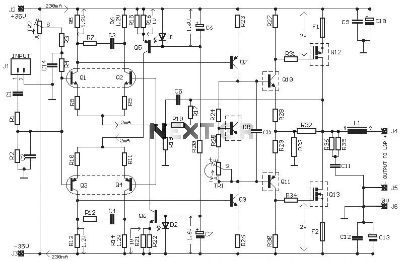
This HEXFET Audio Amplifier 65 Watts circuit diagram includes three circuit images. For a more comprehensive understanding, refer to the original post titled "HEXFET Audio Amp 65 Watts." The post not only provides circuit information but also includes a...
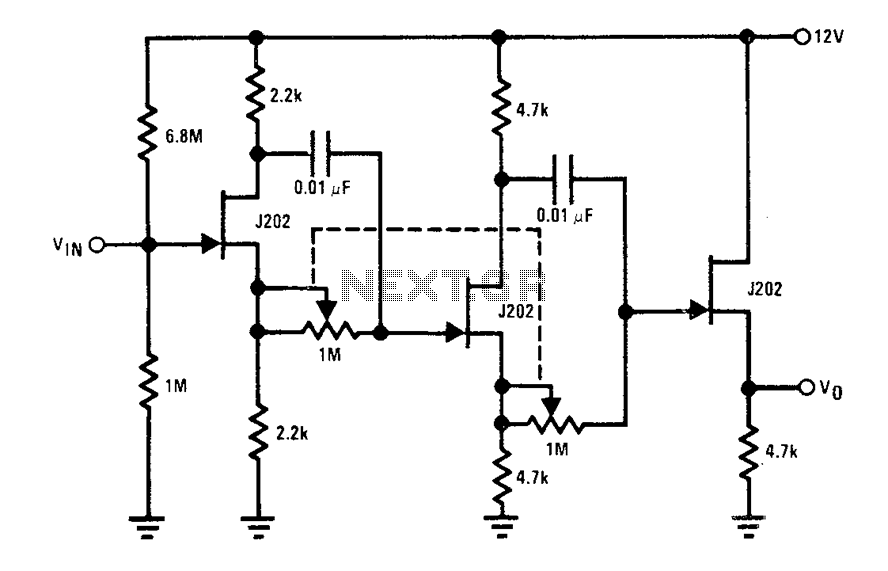
Each J202 JFET stage provides up to 180 degrees of phase shift controlled by a 1 megohm potentiometer. The potentiometer allows for complete control of the groups. JFETs are ideal for the designated circuit because they do not load...
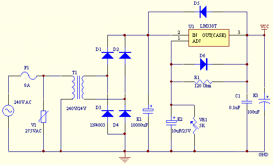
This project utilizes an LM338 adjustable three-terminal regulator to deliver a current of up to 5A with a variable output voltage ranging from 2V to 25V DC. It is particularly useful for powering various electronic circuits during the assembly...
The Mark3 version of the Infrared extender is specifically designed to control appliances that utilize high-frequency modulated infrared remote signals. The Mark3 Infrared extender functions as a bridge between a standard infrared remote control and appliances that operate with high-frequency...
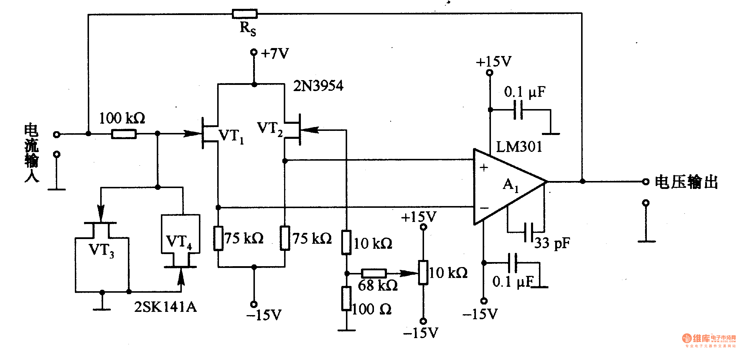
This is a low-input impedance conversion circuit with the reference resistor RS connected to the amplifier's feedback loop, resulting in an input impedance close to zero. The input current flows into the output end of the operational amplifier (Op-Amp)...
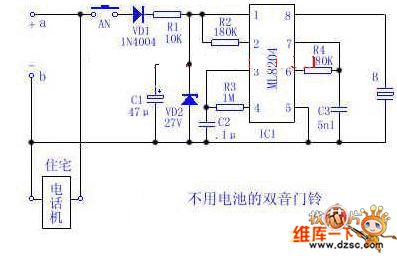
Utilize the 48V (60V) DC feedback electric current supplied by the phone feedback line as the operational energy source for the electronic doorbell, which is highly economical and practical. This document introduces a two-tone doorbell circuit that operates without...