
Inductorless Power Supply Converter Circuit
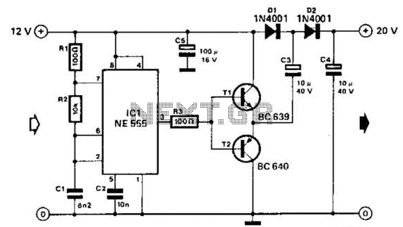
The circuit described utilizes a 555 timer configured in astable mode to generate a square wave signal at a frequency of approximately 8.5 kHz. This oscillating signal serves as the clock input for the subsequent stages of the circuit. The 555 timer is powered by a DC voltage source, and its output is connected to the bases of two transistors, T1 and T2. These transistors are configured as a push-pull amplifier stage, effectively boosting the current output of the 555 timer.
The amplified output from the transistors drives a voltage doubler circuit, which typically consists of two diodes and two capacitors. The voltage doubler works by charging the capacitors during the positive half-cycle of the input signal, and then stacking the voltages during the negative half-cycle, thereby effectively doubling the input voltage. The result is a DC output voltage of approximately 20 V, capable of supplying more than 50 mA of current, making it suitable for various applications requiring higher voltage and moderate current.
It is essential to ensure that the transistors used in the circuit can handle the required current and voltage levels. Additionally, proper heat dissipation measures should be considered to prevent thermal overload. The choice of capacitors in the voltage doubler must also account for their voltage ratings and capacitance values to ensure stable operation and minimal ripple in the output voltage. Using a 555 timer and voltage doubler, this circuit will supply >50mA at 20 Vdc. Tl and T2 act as power amplifiers to drive the voltage doubler. Frequency of operation is approximately 8.5 kHz. 🔗 External reference
Related Circuits
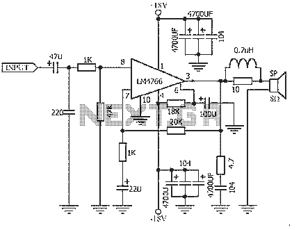
The NS LM4766, launched by a US company, is a two-channel power amplifier integrated circuit. Each channel can output an average power of 40W at an 8-ohm load, with distortion levels lower than 0.1%. It is part of National...
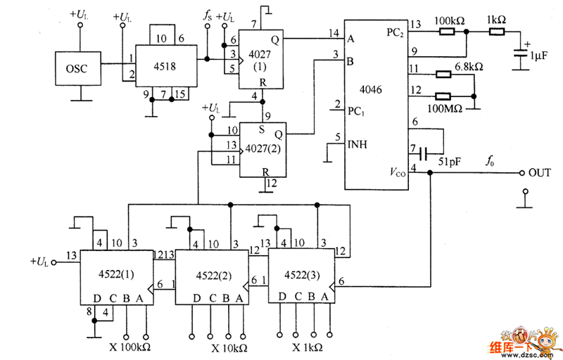
The PLL synthesizer oscillator circuit is a feedback loop consisting of a reference oscillator, phase comparator, loop filter, voltage-controlled oscillator, programmable frequency divider, and various other components. In this circuit, the reference oscillator employs a crystal oscillator (OSC) to...
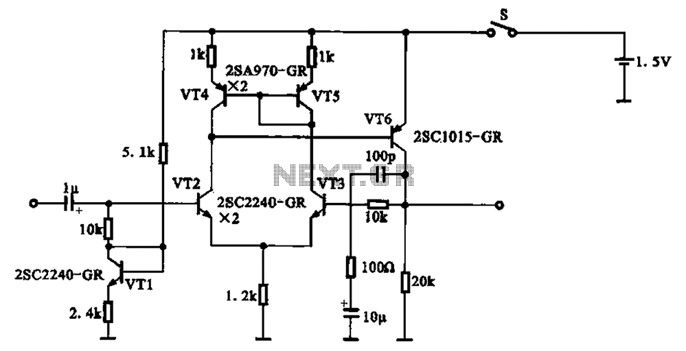
A 1.5V-powered microphone signal amplifying circuit is designed with a power supply for the microphone signal amplification. The circuit primarily consists of a differential amplifier formed by transistors VT2 and VT3. Additionally, VT6 functions as a common emitter voltage...
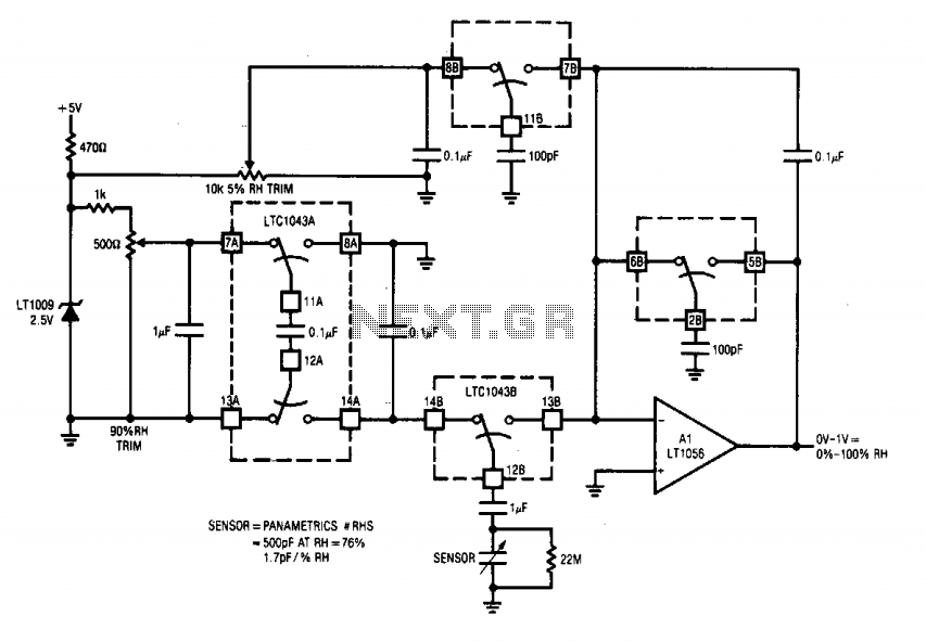
This circuit integrates two LTC1043 devices with a humidity transducer based on a charge-pump configuration. The specified sensor has a nominal capacitance of 400 pF at a relative humidity (RH) of 76%, exhibiting a slope of 1.7 pF/% RH....
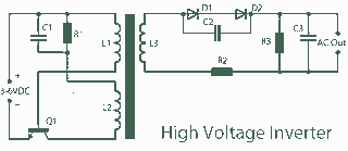
A 3V to 1000V inverter circuit has been constructed, but it is not functioning as intended. The creator seeks expert assistance to identify potential errors in the circuit design. Additionally, there is uncertainty regarding the transformer construction, as the...
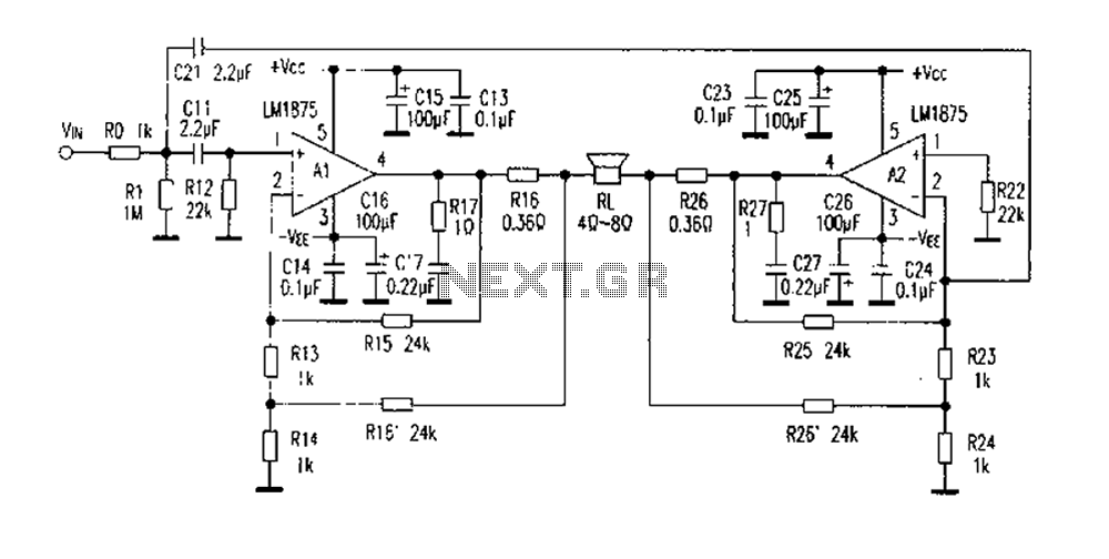
The DC current negative feedback BTL circuit illustrated in Figure 2 eliminates the standard BTL circuit capacitors C12 and C22, which affects the DC characteristics of the circuit. Resistors R16 and R26 function as sampling resistors, while R15, R16,...