
input impedance booster circuit
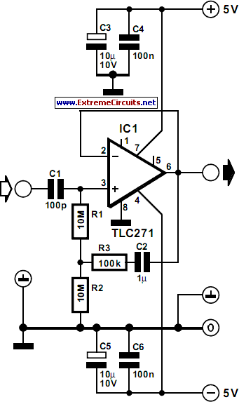
In this AC-coupled op-amp circuit, the input impedance is crucial for maintaining signal integrity and minimizing loading effects on the preceding stage. The choice of resistors R1 and R2 is essential as they not only set the DC operating point but also influence the overall gain and frequency response of the circuit. The feedback mechanism employed in this configuration allows for improved stability and linearity, which are vital for accurate signal amplification.
The bootstrap technique mentioned can involve additional components, such as capacitors and additional resistors, to create a feedback loop that enhances the input impedance further. This is particularly useful in high-impedance applications, such as sensor interfacing, where maintaining a high input impedance is necessary to avoid signal degradation.
In practical designs, careful consideration must be given to the selection of op-amps, as their input bias currents and noise characteristics can significantly impact performance. The specified current draw of approximately 3 mA indicates that the circuit is designed for low-power applications, making it suitable for battery-operated devices or energy-efficient systems.
Overall, the described circuit exemplifies the importance of input impedance in op-amp design and the methods used to achieve high values suitable for various applications in electronic systems.The input impedance of a. c. -coupled op amp circuits depends almost entirely on the resistance that sets the d. c. operating point. If CMOS op amps are used, the input is high, in current op amps up to 10 M. If a higher value is needed, a bootstrap may be used, which enables the input impedance to be boosted artificially to a very high value. In the diagram, resistors R1 plus R2 form the resistance that sets the d. c. operating point for opamp IC1. If no other actions were taken, the input impedance would be about 20M. However, part of the input signal is fed back in phase, so that the alternating current through R1 is smaller. The input impedance, Zin, is then: Zin=(R2+R3)/R3)(R1+R2). With component values as specified, Zin has a value of about 1G. The circuit draws a current of about 3mA. 🔗 External reference
Related Circuits
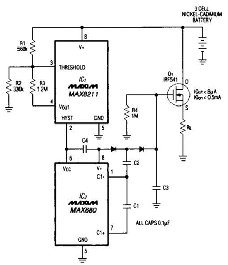
Deep discharge can damage a rechargeable battery. By disconnecting the battery from its load, this circuit halts battery discharge at a predetermined level of declining terminal voltage. Transistor Q1 acts as the switch. The overall circuit draws about 500µA...
This infrared alarm barrier is designed to detect individuals passing through doorways, corridors, and small gates. The transmitter emits an invisible beam of infrared light. When this beam is interrupted by a person, a buzzer connected to the receiver...
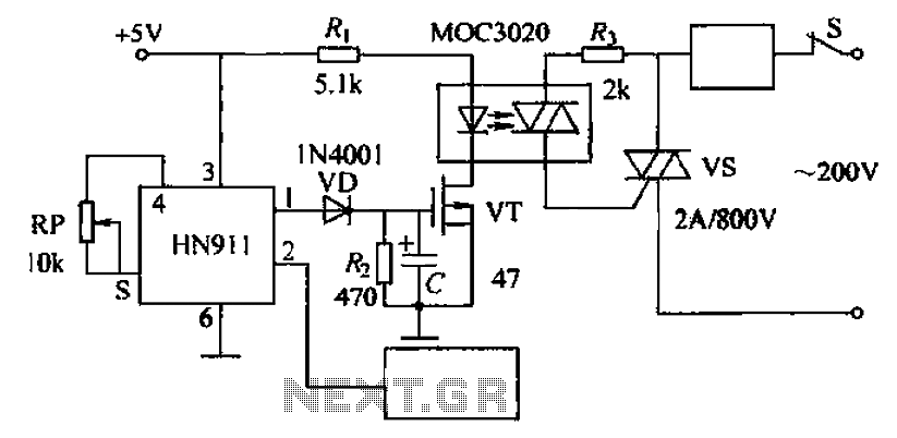
Automatic door control circuit diagram. It utilizes a pyroelectric infrared detection module, HN911, for human motion detection. A variable resistor (potentiometer) is used to adjust the delay time controlled by a transistor (VT). An optocoupler (MX: 3020) provides AC...

A simple USB LED lamp circuit utilizing a 5-volt power supply sourced from a USB port, designed to illuminate a desktop or laptop computer during power outages. The USB LED lamp circuit operates by converting the 5-volt DC power provided...
The low-pass Sallen-Key filter is a staple for designers because it contains few components. By redesigning the filter, a current-to-voltage conversion can be avoided when the input signal to be filtered is in current form. The Sallen-Key filter is a...
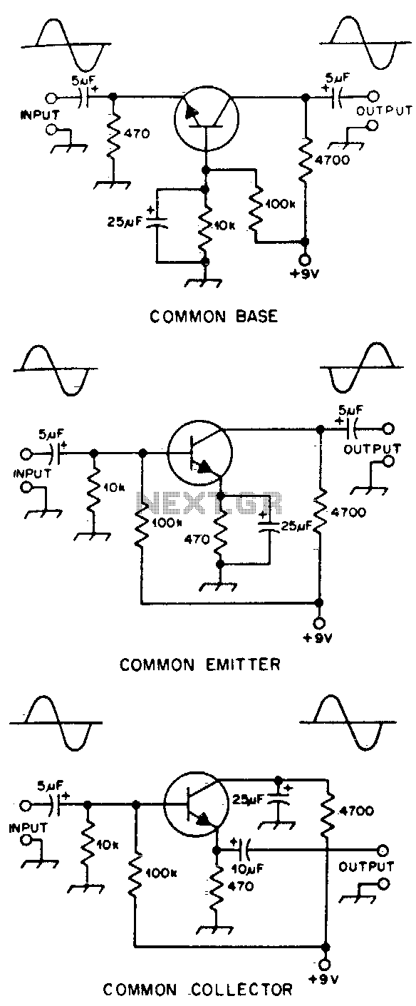
Typical component values are provided for use at audio frequencies, where these circuits are most commonly utilized. The input and output phase relationships are illustrated. The circuit design focuses on audio frequency applications, emphasizing the selection of component values that...