
Load Disconnect Switch Circuit
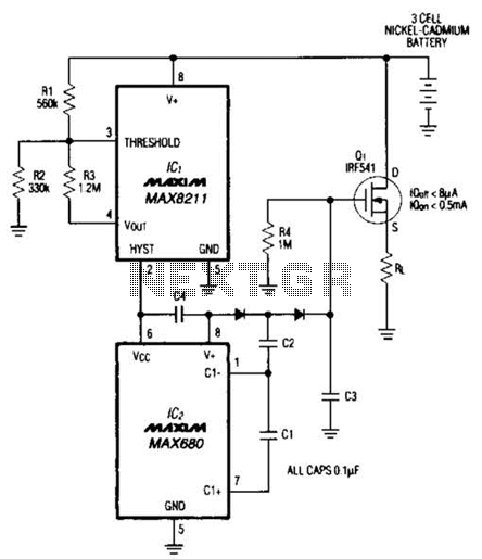
The described circuit is designed to prevent deep discharge of a rechargeable battery, a condition that can lead to irreversible damage and reduced lifespan of the battery. The core component of this circuit is a transistor, designated as Q1, which functions as an electronic switch. The operation of the circuit is based on monitoring the terminal voltage of the battery.
When the battery voltage drops to a specific threshold, indicating a low state of charge, the circuit activates Q1 to disconnect the load from the battery. This action effectively halts any further discharge, preserving the remaining charge in the battery and preventing deep discharge conditions. The circuit is designed to draw a minimal current of approximately 8µA when the switch is open, ensuring that the battery is not subjected to unnecessary drain during idle periods.
Conversely, when the switch is closed, the circuit allows for a higher current draw of about 500µA, enabling normal operation of connected loads. This current draw is essential for the functioning of the circuit's monitoring components, which continuously assess the battery voltage to maintain safe operation.
In practical applications, this circuit can be integrated into battery management systems within devices such as electric vehicles, portable electronics, and renewable energy systems. By implementing this protective circuit, users can significantly enhance the reliability and longevity of rechargeable batteries, ensuring that they operate within safe voltage levels and are not subjected to conditions that could lead to their degradation. Deep discharge can damage a rechargeable battery. By disconnecting the battery from its load, this circuit halts battery discharge at a predetermined level of declining terminal voltage. Transistor Ql acts as the switch. The overall circuit draws about 500A when the switch is closed and about 8 when the switch is open. 🔗 External reference
Related Circuits
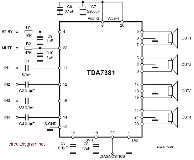
The amplifier is a quad amplifier circuit (amplifier with four inputs and four outputs) based on the TDA7381. This amplifier is designed for car audio systems, but it can also be utilized for other applications. The circuit has a...
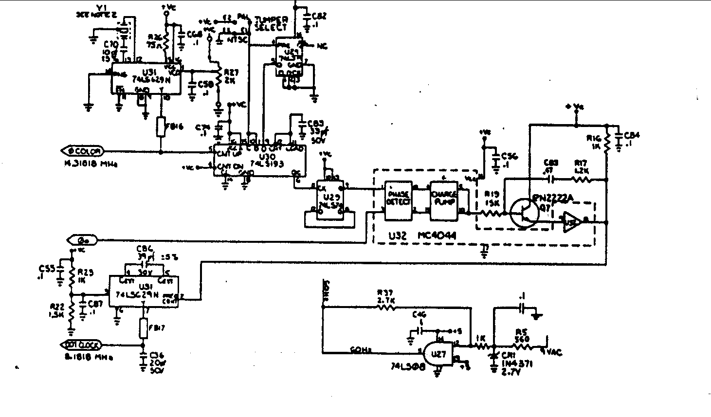
Crystal Y1 generates a fundamental frequency clock signal of 14.31818 MHz. U31 is a Dual Voltage Controlled Oscillator (VCO) that produces a 14.31818 MHz clock signal, referred to as the color clock, at pin 10. The output frequency can...
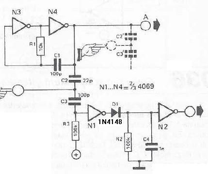
This touch sensor switch is designed using inverters (N1, N2) and several common electronic components. In the standby state, a signal is produced by oscillator N3/N4 at the inputs of N1. When the touch sensor is activated, the hand...
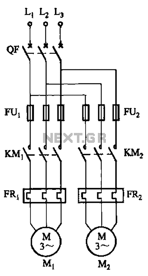
The circuit illustrated in Figure 3-64 operates with switch SA1 in the work position and switch SA2 in the standby position, allowing motor Mi to run while motor Mz remains on standby. In the event of downtime for motor...
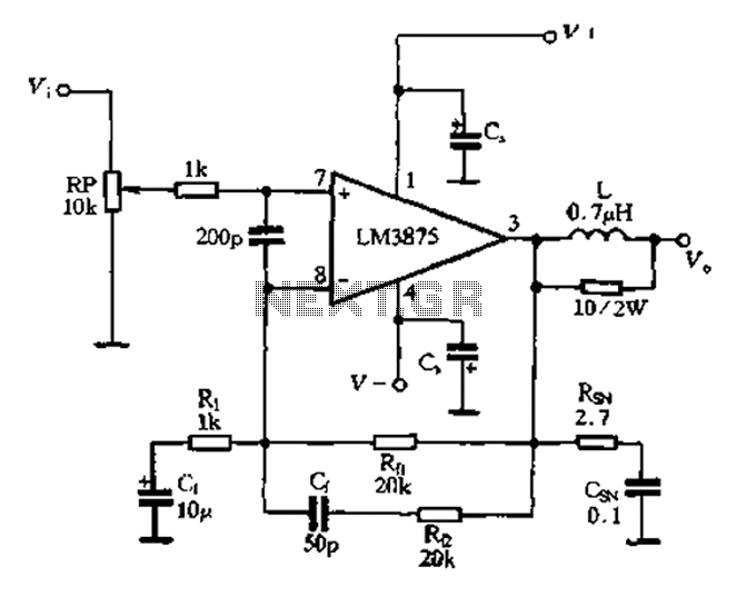
The 875T and LM3876T are high-performance 40W power amplifier integrated circuits (ICs). They operate within a frequency range of 20Hz to 20kHz with a continuous average power output under an 8-ohm load and exhibit a distortion level of only...
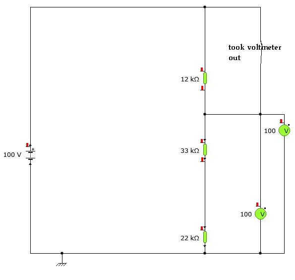
A user is utilizing YENKA software to diagram circuits but is experiencing confusion regarding the voltage calculations in a basic series circuit, as illustrated in the attached image. In a basic series circuit, components are connected end-to-end, forming a single...