
Instrumentation-amplifier
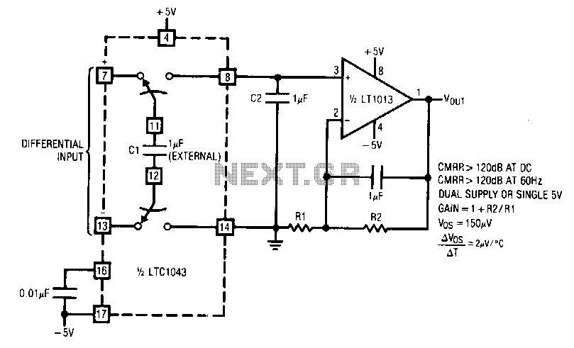
The LTC1043 and LT1013 dual operational amplifiers form the core of a highly efficient dual instrumentation amplifier, which is particularly advantageous in applications requiring precision signal processing. The design employs a single DPDT switch to facilitate the conversion from a differential input to a ground-referenced single-ended output at the LT1013's input stage. This configuration is crucial for enhancing the signal integrity by minimizing noise and interference.
In the operational sequence, when the input switches are engaged, capacitor C1 is charged with the incoming differential signal. This process allows the circuit to accurately sample the input voltage levels. Once the input switches are disengaged, the charge stored in capacitor C1 is transferred to capacitor C2, which is then charged through its own set of switches. The continuous clocking mechanism is essential, as it forces the voltage at C2 to reflect the precise difference between the two input signals, thereby ensuring accurate signal amplification.
The inclusion of a 0.01 µF capacitor at pin 16 is a critical design element, as it determines the switching frequency of the circuit at 500 Hz. This frequency is optimized to balance responsiveness and stability, allowing the amplifier to process signals effectively without introducing significant distortion or delay.
The instrumentation amplifier is designed to exhibit exceptional common-mode rejection, with a ratio surpassing 120 dB. This characteristic is vital in environments where the input signals may be contaminated by common-mode noise, ensuring that only the desired differential signal is amplified. Furthermore, the low drift specification of the circuit contributes to its reliability and accuracy over time, making it suitable for precision measurement applications. Overall, the combination of these features results in a robust and efficient dual instrumentation amplifier capable of delivering high-performance signal processing in various electronic systems.LTC1043 and LT1013 dual op amps are used to create a dual instrumentation amplifier using just two packages. A single DPDT section converts the differential input to a ground-referred single-ended signal at the LT1013"s input.
With the input switches closed, C1 acquires the input signal. When the input switches open, C2"s switches close and C2 receives charge. Continuous clocking forces C2"s voltage to equal the difference between the circuit"s inputs. The 0.01-I"F capacitor at pin 16 sets the switching frequency at 500Hz. Common-mode voltages are rejected by over 120 dB and drift is low. 🔗 External reference
Related Circuits
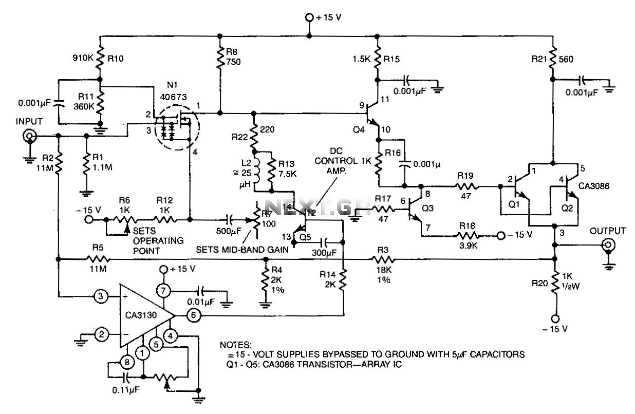
The circuit features an input resistance of 1 MΩ, a bandwidth extending from DC to approximately 35 MHz, and a gain of 10 times. Low-frequency gain is achieved using a CA3130 BiMOS operational amplifier configured as a single-supply amplifier....
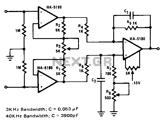
This circuit relies on extremely high input impedance for effective operation. The HA-5180 with its JFET input stage performs well as a preamplifier. The standard three-amplifier configuration is used with very close matching of the resistor ratios R5/R4 and...
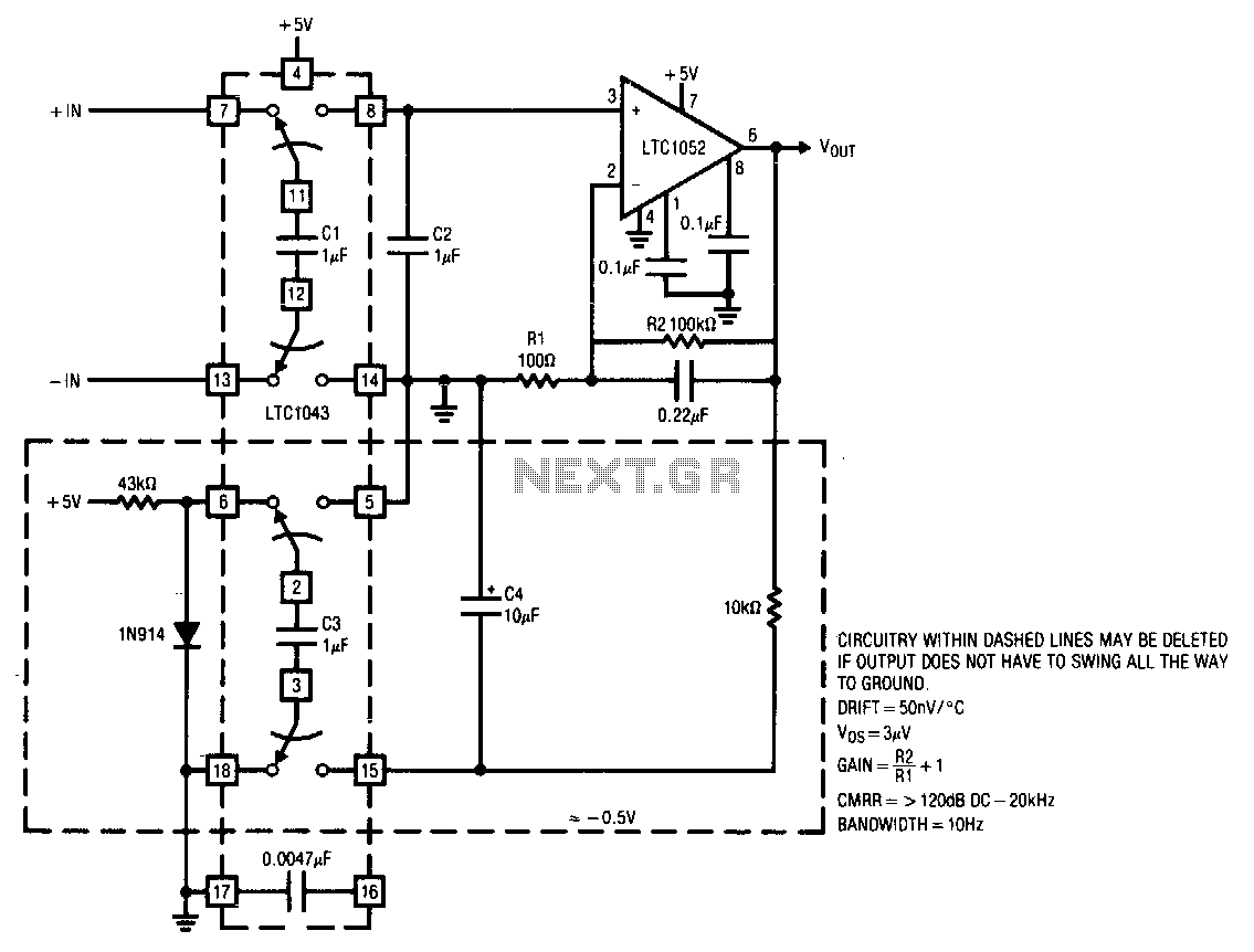
This circuit operates from a single 5 V power supply. The LTC1043 switched-capacitor instrumentation building block facilitates a differential-to-single-ended transition using a flying-capacitor technique. The circuit alternately samples the differential input signal and charges the ground-referred capacitor C2 with...
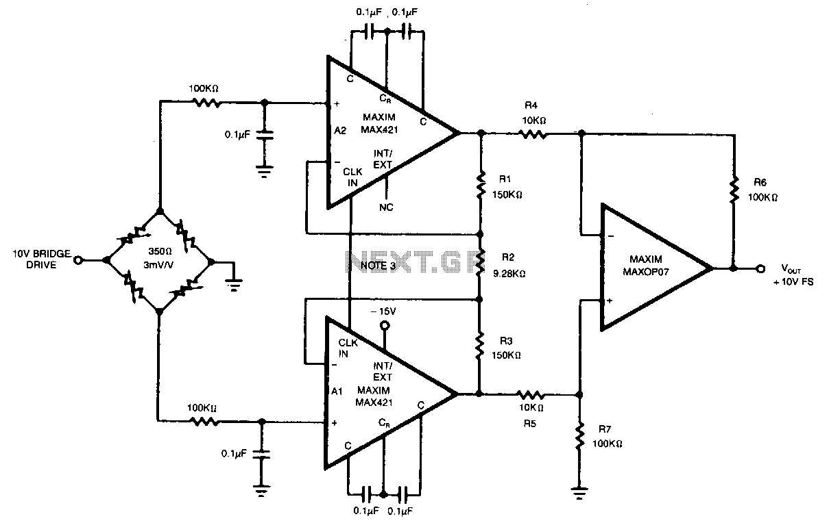
This circuit achieves an overall gain of 320. Additional gain can be obtained by decreasing the value of R2. The untrimmed Vas is 10.11V, and the Vas temperature coefficient is less than 0.1µV/°C. In various applications, the OP07 can...
Warning: include(partials/cookie-banner.php): Failed to open stream: Permission denied in /var/www/html/nextgr/view-circuit.php on line 713
Warning: include(): Failed opening 'partials/cookie-banner.php' for inclusion (include_path='.:/usr/share/php') in /var/www/html/nextgr/view-circuit.php on line 713