
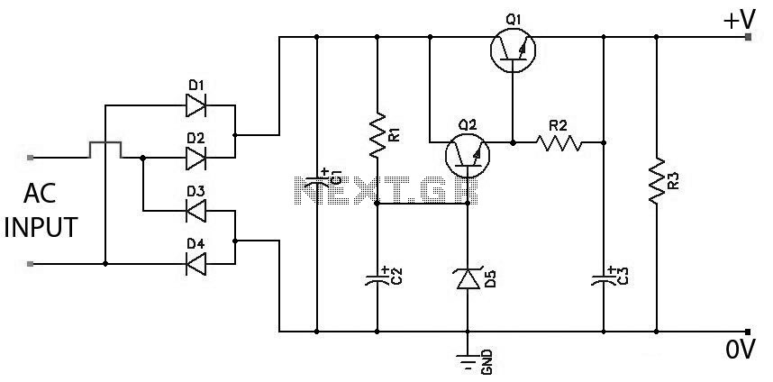
Interfacing High Power Load to Logic Level with Optocoupler
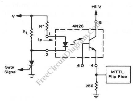
The described circuit utilizes an optocoupler for isolating high power loads from low voltage logic circuits, ensuring safety and signal integrity. The optocoupler consists of a light-emitting diode (LED) and a phototransistor housed in a single package. When a voltage is applied to the LED, it emits light proportional to the input current, which is then detected by the phototransistor. This arrangement allows for electrical isolation between the high power circuit and the low voltage logic circuit, preventing high voltages from affecting sensitive components.
The design of the circuit requires careful selection of the limiter resistor (R*) to optimize performance based on the load's voltage and current specifications. The equation R = V / (0.05 * A) is pivotal in determining the appropriate resistance value, where V is the voltage across the load and A is the current through the LED. This ensures that the optocoupler operates within its specified parameters, providing reliable signal transmission.
For applications involving TTL logic, it is critical that the output current from the phototransistor exceeds 10 mA. This threshold guarantees that the output voltage is sufficient to meet the logic-high requirements of TTL devices, thereby ensuring proper operation of downstream circuitry. Conversely, when interfacing with CMOS logic, the resistor value can be increased to minimize power consumption, thus enhancing the circuit's efficiency.
The schematic diagram accompanying this description visually represents the connections and components involved in the circuit, including the optocoupler, input and output resistors, and any additional protective elements. This comprehensive approach to circuit design enables effective interfacing between high power loads and low voltage logic systems, providing versatility and reliability in various electronic applications.Interfacing high power load can be done in many ways, such as using voltage divider resistors, transformer, or optocoupler. In the circuit shown below, an optocoupler method is presented. This optocoupler serve the logic level translation with flexible input, accepting wide range of voltage level, which is suitable for many high power load/devic
es. To couple a high-voltage load to a low-voltage logic input, this optocoupler basically convert the signal from the load (input) into light internally, and detected by phototransistor inside. The flexibility of the circuit is made possible by changing the limiter resistor (R*) according to the operating voltage of the load, which is determined by following equation: R=V/0.
05*A. To work with TTL loogics, the output current should be greater than 10mA to make sure the output voltage pass the flip-flop`s logic-one level. If dealing only with CMOS logics, then we can increase the 250R resistor to lower the power consumption.
Here is the schematic diagram of the circuit: 🔗 External reference
Related Circuits
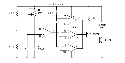
In this circuit, an LM339 quad voltage comparator is utilized to generate a time delay and control a high current output at low voltage. Approximately 5 amps of current can be sourced using a pair of fresh alkaline D...
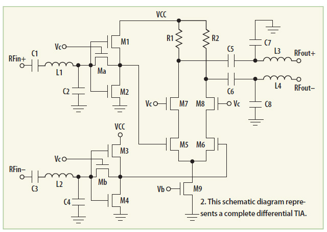
This transimpedance amplifier utilizes a current-reuse stage and a cascaded differential stage to provide a continuous gain tuning range of 15 dB, along with a low noise figure of 1.061 dB at 2.4 GHz. The transimpedance amplifier (TIA) is designed...
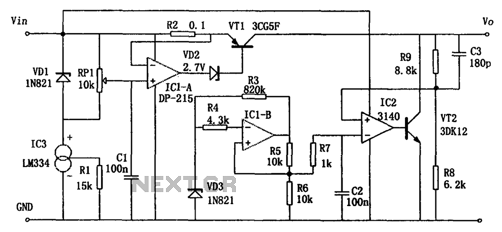
The circuit functions as a switching power supply designed to operate alongside a linear regulated power supply. Key characteristics include high efficiency and low dropout voltage. It effectively filters out high-frequency ripple voltage and manages instantaneous voltage variations, making...
Low Ripple Regulated Power Supply Circuit Diagram. This circuit can be employed in applications requiring high current with minimal ripple voltage, such as in high-powered class AB amplifiers where high-quality audio reproduction is essential. The low ripple regulated power...
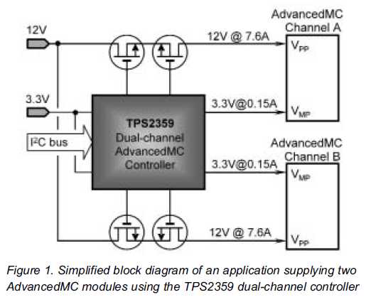
The new TPS2359 hot-plug controller integrates all power management functions for two AdvancedMC (AMC) modules. Its current limiting circuitry enables designers to meet stringent AMC requirements, particularly in applications utilizing redundant supplies. A unique feature called multiswap maintains a...
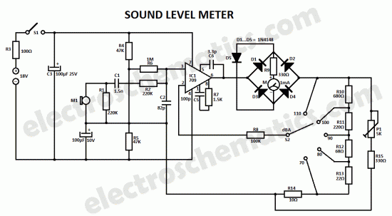
This sound level measuring device circuit can be used to control the intensity of a sound recording in the field of a disco. It has five measurement ranges between 70 and 120 dB, with a measurement accuracy of 0.5...