
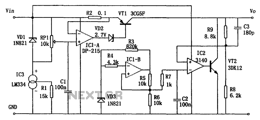
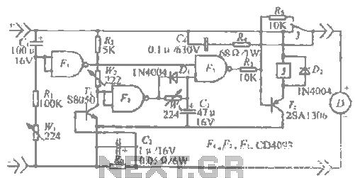
High-performance power supply LM334
The switching power supply circuit described is characterized by its ability to efficiently convert input voltage to a stable output voltage while minimizing power loss. The integration of the linear regulated power supply allows for enhanced performance in applications requiring precise voltage regulation. The circuit's high efficiency is particularly advantageous in battery-powered devices, where energy conservation is critical.
The voltage sampling circuit, comprising resistors R8 and R9, plays a crucial role in monitoring the output voltage. By providing feedback to the error amplifier, this arrangement ensures that any fluctuations in output voltage are promptly addressed. The error amplifier, formed by IC2 and VT2, amplifies the difference between the reference voltage and the sampled output voltage, adjusting the control signal to maintain a consistent output.
Moreover, the current limiting feature is essential for protecting the circuit from overload conditions. The adjustable reference voltage generated by IC1-a allows for flexibility in setting the maximum allowable output current. This is particularly useful in applications where varying load conditions may lead to excessive current draw. The output current is sampled through resistor R2, and the resulting voltage is compared to the reference voltage to produce an error voltage. This error voltage is utilized to modulate the operation of regulator VT1, ensuring that the output current remains within safe limits.
Overall, the described circuit is well-suited for applications requiring reliable power delivery with stringent voltage and current specifications. Its design effectively balances performance with safety, making it a valuable component in modern electronic systems. As shown in Figure as a switching power supply to work with linear regulated power supply. Its characteristics are: high efficiency, low dropout; having the ability to filter o ut high frequency ripple voltage and instantaneous voltage of the mutation; best suited to the needs of small loads; having a current limiting function. Figure by VD3, IC1-b and other components to generate the reference voltage. R8, R9 constitute a voltage sampling circuit for sampling the output voltage of the power supply. IC2 and VT2 and other elements constituting the error amplifier and shunt voltage regulator circuit. By comparing the reference voltage and IC2 amplify the sampled voltage, the driving regulator VT2, thereby stabilizing the output voltage.
By the VD1, IC3, VD2, IC1-a, VT1 and other elements constituting a current limiting circuit. VD1, IC3 and RP1 formed adjustable current limiting reference voltage generated by IC1-a reference to this voltage R2 (output current sampling resistor) comparing the sampled voltage amplification to form the error voltage. With the error voltage control the regulator VT1 working conditions, so as to stabilize and limit the output current.
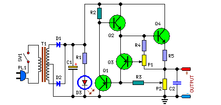
Related Circuits
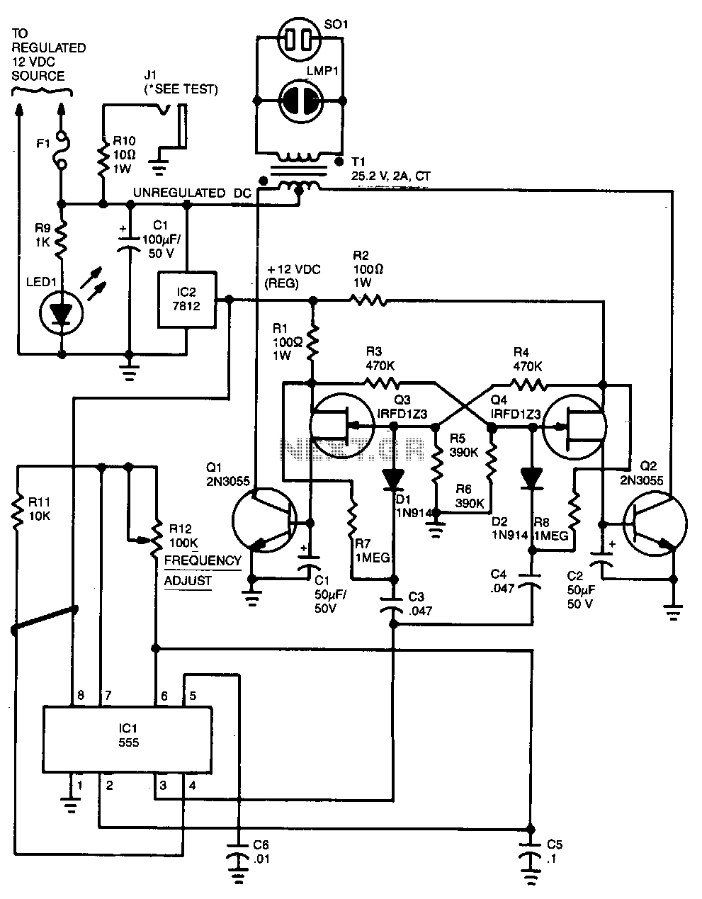
Capacitor C5 and potentiometer R12 determine the frequency of the output signal at pin 3 of IC1, the 555 oscillator. The output signal is differentiated by C3 and C4 before it is input to the base of power transistors...
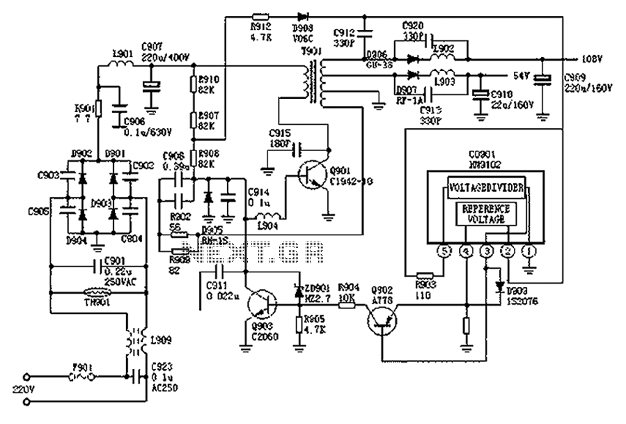
The Hitachi NP8C switching power supply circuit is illustrated in FIG. The Hitachi NP8C power models include CTP236, CEP320D, CRP350D, 450D, Furi HFC-236, 450, and Venus C37-401, C46-1, C563, among others. This circuit was widely used in early Chinese...
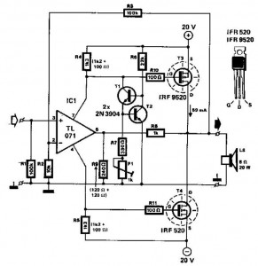
This audio power amplifier employs two complementary MOSFETs (IRF9520 and IRF520) to provide up to 20W output into an 8-ohm speaker. A TL071 operational amplifier functions as the input amplifier. The MOSFETs require heatsinking with a thermal resistance of...
The "R-h sampling circuit limit order" aims to reduce the sampling resistor. A DC voltage level can be positioned between the components. The circuit includes a line amplifier that allows for magnification adjustments and is designed to protect against...
The transformer can be selected based on the required maximum voltage and current output. Recommended options include: 36V, 40V, or 48V center-tapped configurations, with power ratings of 50VA, 75VA, 80VA, or 100VA. It is essential to mount Q4 on...
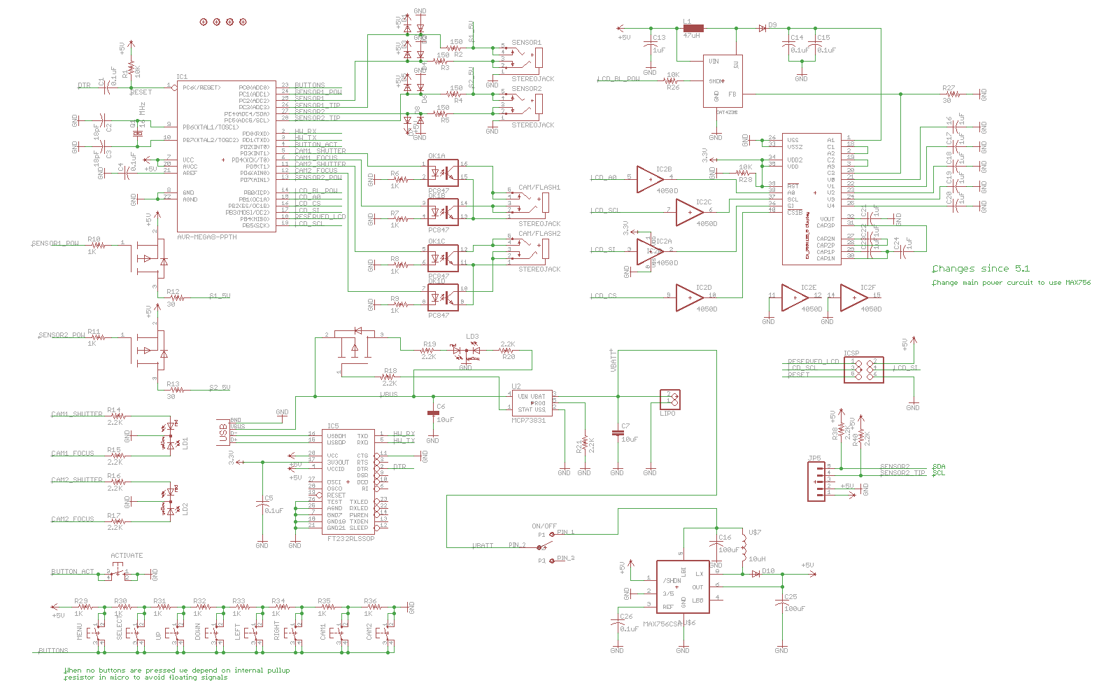
Previously, a linear regulator was used, but a Max756 boost converter is now in operation. An output ripple of 0.1 to 0.3V is observed in the current, while the Max756 datasheet indicates an expected ripple of about 50 mA....