
Introduction to PWM Inverters
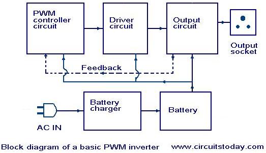
This process involves feeding back a portion of the inverter's output to the PWM controller section (PWM controller IC). Based on this feedback voltage, the PWM controller makes necessary adjustments to the pulse width of the switching pulse generated by the oscillator. Consequently, this alteration in pulse width counteracts output voltage changes, ensuring a stable inverter output despite load variations. Additionally, a circuit monitors the charging current of the battery to maintain it within the rated value, as excessive or insufficient charging current can adversely affect battery lifespan. This circuit also measures battery voltage to initiate charging when the battery is depleted and to transition to trickle charging once the battery is fully charged.
Furthermore, a circuit detects the availability of AC mains power, placing the inverter in charging mode when AC mains is present and in battery mode when it is absent. A delay circuit is implemented to postpone battery charging by 8 to 10 seconds after power restoration, protecting the MOSFETs from high currents resulting from immediate charging. This feature is commonly referred to as Mains Delay. An overload monitoring circuit tracks the inverter's output current; if the output current exceeds the rated value, it signals the shutdown circuit to indicate an overload condition. The shutdown circuit continuously monitors the inverter's operation and will deactivate it in the event of any abnormalities.
The outputs from various sensor circuits serve as inputs to the inverter. The PWM controller circuit regulates the inverter's output voltage, typically utilizing a single PWM IC such as KA3525 or LM494, which integrates all necessary circuits for PWM operation. The battery charging circuit manages the battery charging process, taking inputs from the AC mains sensing circuit and the battery voltage sensor circuits. A driver circuit, which may consist of transistors or specially designed driver ICs, controls the output section of the inverter according to the switching frequency. This driver circuit functions similarly to a preamplifier. The output section drives the load and includes a step-up transformer to elevate the battery voltage to line voltage, alongside an array of switching MOSFET devices that drive the primary side of the step-up transformer. The output voltage is then available at the secondary winding of the transformer.Now a days most of the inverters available in the market utilizes the PWM(Pulse Width Modulation) technology. The inverters based on PWM technology are superior in many factors compared to other inverters designed using conventional technologies.
The PWM based inverters generally use MOSFETs in the output switching stage. In such cases the inverters are generally termed as PWM MOSFET inverters. The inverters based on PWM technology has a lot of protection and control circuits compared to the traditional inverters. PWM or Pulse width Modulation is used to keep the output voltage of the inverter at the rated voltage(110V AC / 220V AC) (depending on the country) irrespective of the output load.
In a conventional inverter the output voltage changes according to the changes in the load. To nullify effect caused by the changing loads, the PWM inverter correct the output voltage according to the value of the load connected at the output. This is accomplished by changing the width of the switching frequency generated by the oscillator section.
The AC voltage at the output depend on the width of the switching pulse. The process is achieved by feed backing a part of the inverter output to the PWM controller section (PWM controller IC). Based on this feedback voltage the PWM controller will make necessary corrections in the pulse width of the switching pulse generated at oscillator section.
This change in the pulse width of the switching pulse will cancel the changes in the output voltage and the inverter output will stay constant irrespective of the load variations. This circuit senses the charging current of the battery in order to keep the charging current with in the rated value.
A charging current lower or higher than the allowed range can reduce battery life. This circuit senses the battery voltage in order to charge the battery when the battery is exhausted and to start trickle charging the battery when it is fully charged. This circuit senses the availability of AC mains. When AC mains is available the inverter will be in charging mode. When AC mains is not available the inverter will be in battery mode. This circuit delays the charging of the battery 8 10 seconds after the power is resumed. This is generally used to protect the MOSFETS from high currents generated as a result of immediate charging.
This mechanism is also termed as Mains Delay Over load monitors the output current of the inverter. If the output current increases above the rated value, it will send a signal to the Shut down circuit indicating that there is an overload. Shutdown circuit closely monitors the inverter and shuts it down when any abnormality occurs. The out put from the various sensor circuits are the input to the inverter. PWM controller circuit regulate the output voltage of the inverter. Usually a single PWM IC such as KA3525 or LM494 are used for the purpose. The entire circuits needed for the PWM operation will be incorporated in such ICs. Battery charging circuit controls the charging process of the battery. The output of AC mains sensing circuit and Battery voltage sensor circuits are the inputs for the battery charging circuit.
Driver circuit drives the output section of the inverter according to the switching frequency. Transistors or Specially designed driver ICs are employed in the driver circuit. The driver circuit is some what similar to a preamplifier. Output section drives the load. It consists of a step up transformer for stepping up the battery voltage to the line voltage and an array of switching MOSFET devices for driving the primary of the step up transformer. The output voltage will be available at the secondary of the step up transformer. 🔗 External reference
Related Circuits
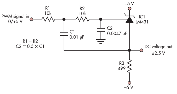
This simple circuit converts a 5V PWM signal into a variable precision reference voltage with a range of -2.5V to +2.5V. Many designs, such as a digitally controlled power supply or a programmable dummy load, require a Digital to...
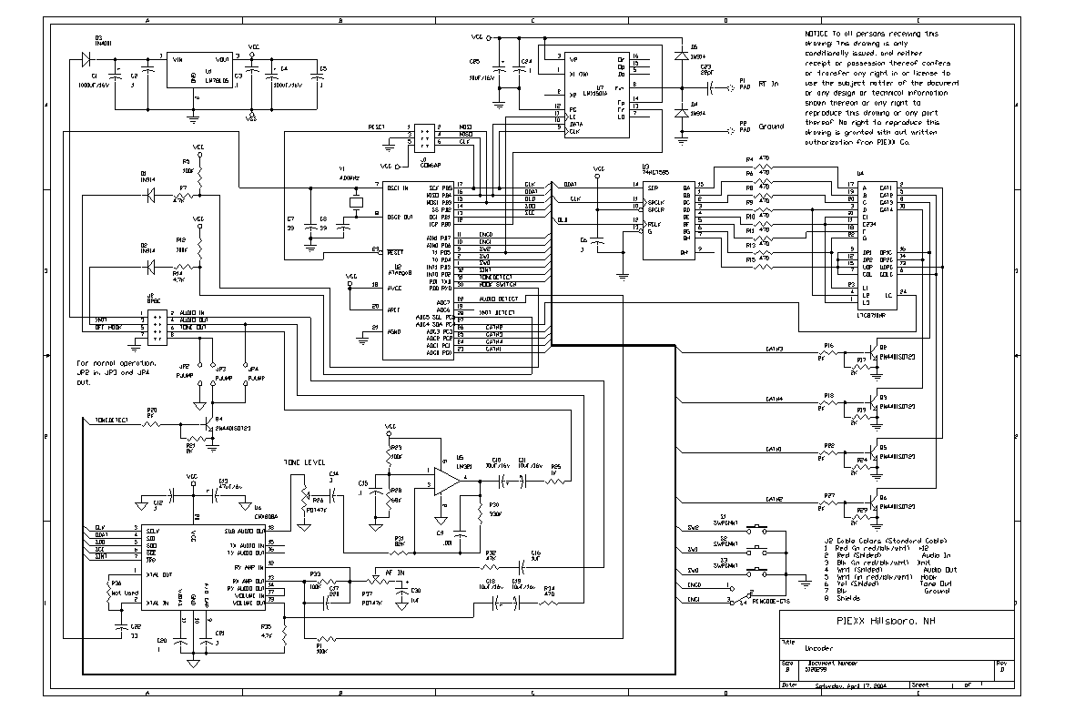
What can be done with old 2-Meter FM rigs that lack CTCSS tone capability? The solution is to add a tone encoder. Traditional tone encoders require knowledge of the repeater's tone and necessitate manual adjustment every time a different...
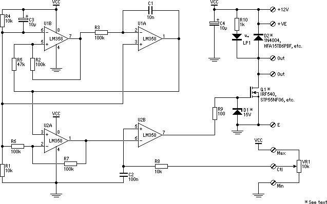
This project addresses the need for a simple circuit that can dim LED lights or control the speed of 12V DC motors. The circuit utilizes Pulse Width Modulation (PWM) to manage the effective or average current flowing through an...
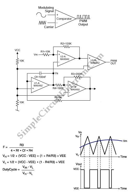
This is a simple PWM modulator circuit. Comparing the message signal to a ramp or triangular waveform is the simplest way to produce a PWM signal. When the... The PWM (Pulse Width Modulation) modulator circuit operates by comparing a modulating...
This is a Class D audio amplifier circuit used to control the PWM motor speed. This circuit has two advantages for battery-powered portable devices. First, it provides high efficiency, which extends battery life. The Class D audio amplifier operates by...

The circuit described is a crystal oscillation circuit using a CM OS inverting configuration, designed to ensure accurate operation. It employs a BCD counter (IC2) capable of achieving a maximum oscillation frequency of 2 MHz, which is 100 times...