
Keyer circuit
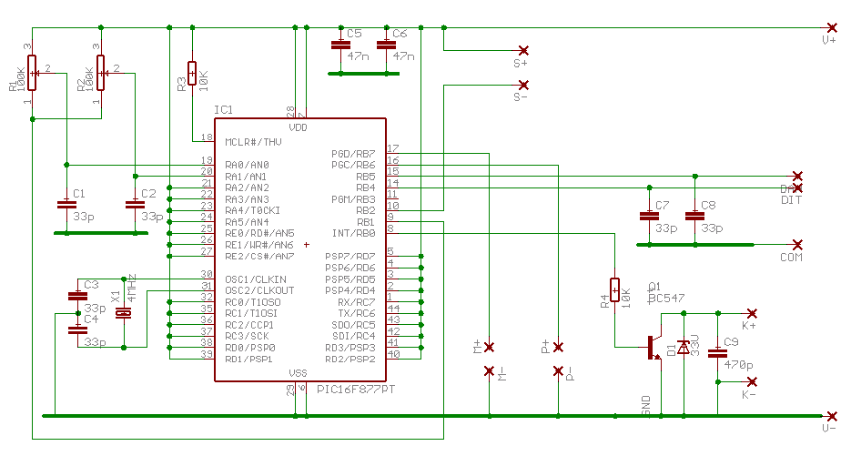
The circuit schematic utilizes the PIC16F877A microcontroller as the primary processing unit, which is well-suited for applications requiring efficient processing of Morse code signals. The microcontroller's architecture includes multiple I/O pins that facilitate the connection of user interface components such as the dit and dah paddles, as well as the menu and memory buttons. The use of a 4MHz oscillator ensures stable operation while minimizing potential layout issues that could arise from higher frequency components.
The power supply design, utilizing three AA batteries, is a practical choice for portable applications, and the implementation of a power switch allows for user control over device activation. The sleep mode feature of the PIC16F877A is crucial for extending battery life, as it significantly reduces power consumption during periods of inactivity.
Decoupling capacitors C5 and C6 are strategically placed to stabilize the power supply lines, minimizing noise and ensuring reliable operation of the microcontroller. The oscillator circuit, consisting of a ceramic resonator, is critical for maintaining the timing accuracy necessary for Morse code generation and decoding.
The inclusion of resistors R1 and R2 as adjustable controls for speed and weight enhances user customization, allowing operators to tailor the keyer's response to their preferences. The interrupt capability of pins RB4 to RB7 is a vital feature, enabling the device to respond promptly to user inputs, even when in a low-power state.
The output stage, driven by transistor Q1, is designed to interface with standard transmitter key inputs, ensuring compatibility with a wide range of radio equipment. This design approach provides flexibility for users who may require different voltage levels or signaling protocols.
Overall, the circuit schematic represents a comprehensive and efficient design for a Morse code keyer, integrating user-friendly features with robust electronic components to deliver reliable performance in a compact form factor.A larger version of the circuit diagram by clicking here. The circuit was drawn using Eagle from CadSoft, a schematic and PCB layout package that is free to use for small non-commercial projects. The heart of the keyer is the PIC16F877A chip. This is a 20MHz microcontroller with a generous amount of I/O capability including up to 8 A DC`s on board with resolutions of 10 bits each. Power to the chip is obtained by 3 x AA cells in series and a power on/off switch is used. Even with the power left on, the sleep mode of the PIC chip reduces current draw to negligible amounts. C5 and C6 are used to decouple the VSS and VDD lines of the chip, one on either side close to the pins.
X1, C3 and C4 form the oscillator circuit and in this case a 4MHz ceramic resonator is used which is well below the 20MHz maximum rating of the chip. The lower frequency was chosen to prevent any layout problems on the stripboard, and 4MHz still results in a throughput of one million instructions per second plenty for a morse keyer.
R1 and R2 are the speed and weight controls respectively. These are commoned on the VDD line, although the tails are taken to the RB1 pin on the chip. RB1 is normally held at logic 1 so that no current flows through the pots, assisting with the low current drain for battery operated equipment. RB1 is pulsed low to read the pots and does so continuously while operating. Pins RB4 to RB7 are the four inputs for the dit and dah paddles, and the menu and memory pushbuttons.
The significance of using these pins is that they can generate an interrupt and wake the device up from sleep mode. This is of critical importance as the PIC device is sent to sleep even between characters. Finally, Q1 drives the key input of the transmitter or transceiver limited to 33V and 100mA. It is assumed that the key input of the TX is some positive voltage which is shorted to ground by the key .
If negative voltages are used, or a different protocol, then changes are necessary to this area. Pressing the menu button invokes the menu mode. It will stay in the menu mode for up to 5 seconds, then timeout with dit meaning E for Exit. Pressing the menu button again will take it out of the menu. Key in dah-dah and the keyer will respond with N to indicate a number is needed. Valid entries are dit-dah-dah-dah-dah, dit-dit-dah-dah-dah or dit-dit-dit-dah-dah. Shortcuts are dit, dit-dit, and dit-dit-dit respectively. Records over the current memory. Key in dit-dah-dit and the keyer will respond with R to signify record mode. Record the message on the paddles and stop, the keyer will automatically recognise the end of the message and respond with K. Up to 64 characters can be recorded. Key in dah and the sidetone will be changed from its current setting. The keyer will respond with Y or N depending on whether the sidetone is on or not. The sidetone is always on during menu operations, even if switched off with T. These pages and contents are Copyright ©2004-2014 Duncan Munro M0KGK. All trademarks used herein are acknowledged. Email any queries about these pages to postmaster@duncanamps. com 🔗 External reference
Related Circuits
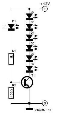
Its state is constantly changing, and this change affects the flow of current and voltage, which is visible with the two LEDs. The speed of the LED flasher can be adjusted with potentiometer P1. As an astable multivibrator, the...
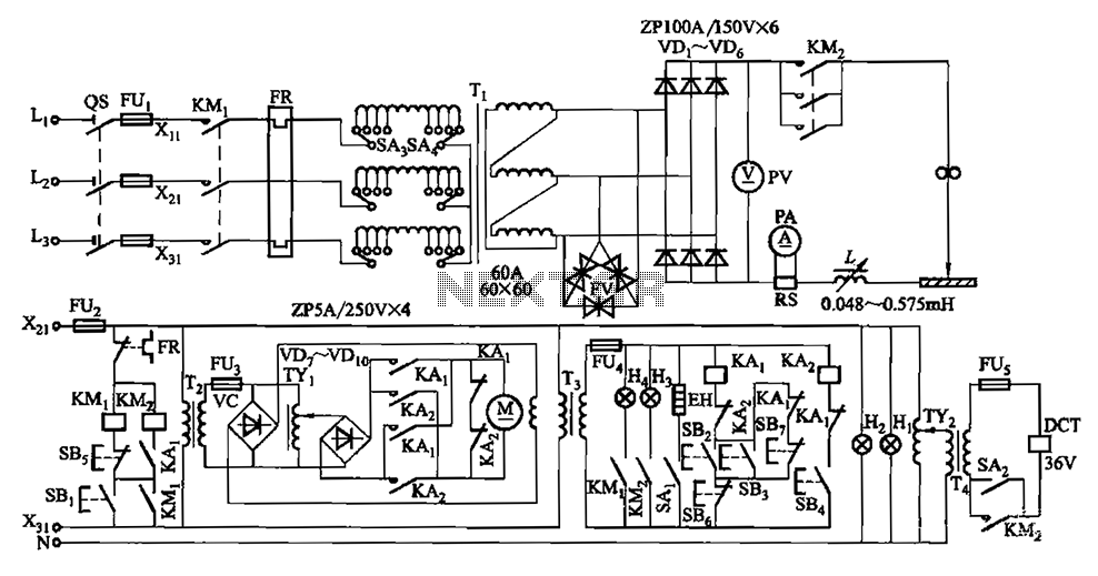
CO2 gas shielded arc welding power supply electromagnetic vibration circuit is commonly used in farm machinery repair. The maximum arc voltage is 30V, with a maximum welding current of 300A. The wire feed speed ranges from 0 to 12...
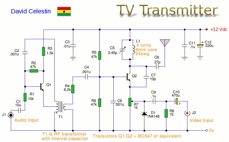
This is an analog TV transmitter. Sound modulation is of the FM type with a 5.5 MHz carrier frequency, and video transmission follows the PAL standard. The frequency can be adjusted using capacitor C5, allowing tuning from 54 to...
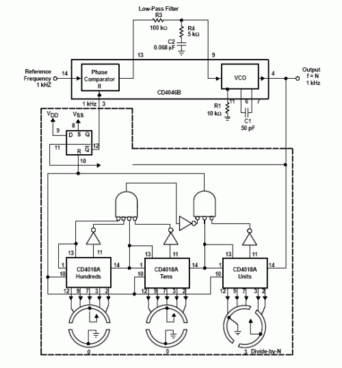
A frequency synthesizer circuit diagram has been found, but clarification is needed regarding a component connected to VDD from pin 9, VSS from pin 8, and pin 12, which is linked to the phase comparator 2. The component in...
A relay control circuit is illustrated, which is commonly found in microwave switches. This circuit facilitates the operation of various components such as the power supply switch, electric fans, light bulbs, food turntables, and timers. The relay control signal...
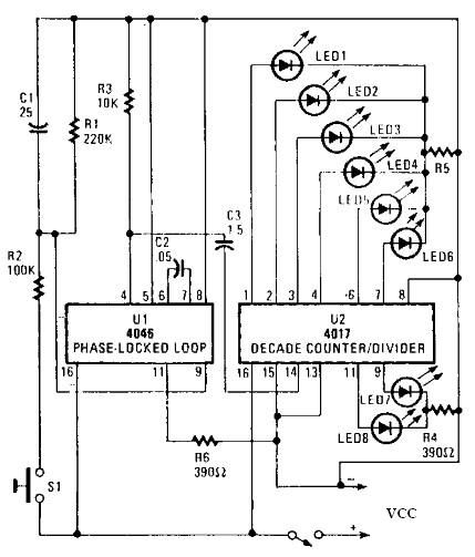
An electronic circuit for a roulette wheel can be constructed using a 4046 Phase-Locked Loop (PLL) that includes a Voltage Controlled Oscillator (VCO), two phase comparators, a source follower, and a Zener diode to generate a low-frequency pulsed output...