
LC inductance / capacitance meter
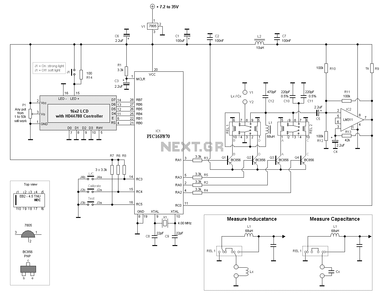
The LC meter design utilizes an LC oscillator configuration based on the LM311 comparator, which serves as the core component in generating oscillating signals for measuring inductance and capacitance. The primary components of the circuit include a PIC16F870 microcontroller, a 4 MHz crystal oscillator, and a 16-character LCD display, which is interfaced in a 4-wire mode. The oscillator output is taken from pin 7 of the LM311 and fed into pin 11 of the PIC, allowing the microcontroller to process the frequency information.
The circuit incorporates two relays, REL1 and REL2, which facilitate automatic measurement functions while minimizing stray inductance and capacitance. REL1 is designed to switch between measuring inductance and capacitance. In inductance measurement mode, REL1 connects the unknown inductor (Lx) in series with a known inductor (L1), while in capacitance mode, it connects the unknown capacitor (Cx) in parallel with a reference capacitor.
REL2 is dedicated solely to adding a reference capacitor during calibration, ensuring accurate measurement results. Supporting components such as capacitor C4 and resistor R13 are included to stabilize the oscillator's startup process.
The design also features provisions for user interaction through three buttons for selecting measurement modes (L/C), initiating calibration, and testing inputs. The power supply circuit includes inductance L2 and capacitance C7, which work together to filter out RF noise and provide a stable power supply to the circuit.
A jumper (J1) is incorporated to control the LCD backlight intensity. When disconnected, the LCD operates with a soft backlight due to lower current passing through resistor R14; when connected, the backlight is intensified.
Grounding is crucial in RF applications, and the design employs a dual-layer PCB with a dedicated ground plane on the bottom layer. Connections between the top and bottom layers are made through three via-holes labeled "GND," ensuring a robust grounding scheme. Additionally, the assembly process requires careful drilling of holes for a 2.54 mm pin header to connect the LCD, ensuring no copper traces connect to the header on the back side of the PCB. This is achieved by using a larger drill bit to remove copper from the back, maintaining the integrity of the ground plane.LC-meter will work equally good with or without your knowledge about the theory. The LC meter is actually an LC oscillator based around the familiar comparator circuit LM 311. I have not changed the LC oscillator much from others projects, since this is an excellent oscillator. The main part of this project is a LCD, PIC16F870 and an oscillator LM311. The LCD is a standard 2 line 16 chars display connected in 4-wire mode to the PIC. At the bottom you will find a 4.000 MHz crystal to run the PIC. The heart of this construction is the LC oscillator based around IC2. The frequency pops out at pin 7 and then enters the PIC at pin 11. Two relays have been added to make the measurement more automatic, and they will also prevent stray inductance/capacitance.
The two relays are controlled by 4 transistors. The reason why I choose this construction was to keep the current consumption to a constant low level. If the current fluctuates, it will affect the measurement which is not good. The relays I use are a bit different since they have "double-coil latch types". REL1 choose to measure between Inductance or Capacitance. (see bottom of schematic). When you measure inductance, REL1 will add the unknown inductor Lx in serial with L1. When you measure capacitance, REL1 will add the unknown capacitor in parallell with Cx. REL 2 has only one function and that is to add the reference capacitor during the calibration phase. C4, R13 is added to make sure the oscillator starts up correctly. At the left side of the schematic you find the LCD display and you will also find three inputs. You should connect 3 buttons to the unit. (L/C, Calibration, Test input) L2 and C7 is added to make the power line smooth and reject RF. A jumper J1 is added to choose if you want strong backlight or not. If jumper J1 is disconnected the LCD will have soft backlight because a low current will pass through R14.
If jumper J1 is connected you will have strong backlight. Good grounding is very important in a RF system. I use bottom layer as Ground and I connect it with the top layer at three places (via-holes) to get a good grounding. Drill a small hole through the PCB and solder a wire in each via-hole to connect the top layer with the bottom layer which is the ground layer.
The three via-holes can easy be found on the PCB and in the assembly pic at right, they are labelled "GND" and marked with red colour. Drill the remaining 16 holes for the Pin Header 2.54mm which will connect the LCD to the PCB. Since the backplane of the PCB is Ground you must make sure there is no connecting copper to the Pin Header 2.54mm at the backside.
Easiest way is to remove the copper at the backside is to use a larger drill (3mm) and drill a bit in the holes at the backside of the PCB. 🔗 External reference
Related Circuits

This circuit is designed to measure the voltage of a 12V nominal lead-acid rechargeable battery system. While it was specifically created for solar-powered systems, it is versatile enough for use in automotive or other 12V applications. Lead-acid batteries typically...
A field strength meter is highly valuable when working with RF devices. It can quickly diagnose whether a transmitter circuit is functioning and detect RF signals in the environment. The simplest form of a field strength meter can be...
A simple electronic multimeter offers an affordable alternative for hobbyists deterred by the high cost of conventional multimeters. This device is designed to measure three ranges: (i) 0-15V, (ii) 0-15mA, and (iii) 0-150mA, with the possibility of extending the...

A simple audio watt meter circuit or an audio power or audio level meter circuit with diagram and schematics to measure amplifier audio output power in watts. The audio watt meter circuit is designed to measure the output power of...
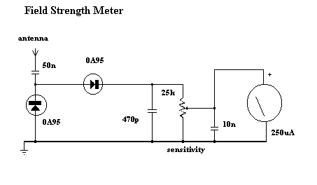
Because it uses few parts, a printed circuit board is not necessary; components can simply be soldered to one another. However, a box is desirable for operating convenience. The case and aerial from a discarded toy walkie-talkie was used...
It is advisable to modify inexpensive USB speakers to obtain a pre-assembled analog front-end for this project. If this is not feasible, then soldering will be necessary, requiring a minimum of two resistors and one capacitor, assuming the display...