
Lc Sine-Wave Generator
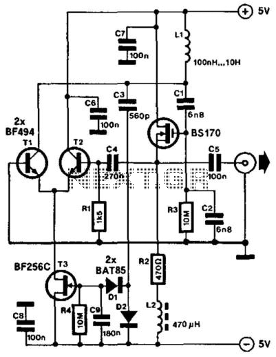
The compact LC oscillator circuit is designed to generate a stable sine wave output across a broad frequency spectrum, making it suitable for various applications, including signal generation and testing. The series-resonant circuit configuration ensures that the desired frequency can be precisely tuned by adjusting the values of L1, C2, and C3. The use of a common base amplifier configuration for T1 allows for high-frequency operation with minimal phase shift, which is crucial for maintaining signal integrity at high frequencies.
The feedback mechanism implemented in this oscillator is critical for sustaining oscillation. The capacitive divider formed by C1 and C2 plays a pivotal role in determining the feedback ratio, which directly influences the oscillator's stability and output amplitude. The incorporation of a source follower (BS170) further enhances the circuit's performance by isolating the feedback network from the output stage, preventing loading effects that could destabilize the oscillation.
The amplitude control feature is particularly noteworthy, as it allows for dynamic adjustment of the output signal level. By rectifying the output and using it to control the biasing of T3, the circuit can adaptively respond to varying input signal levels, ensuring consistent output quality without distortion. This is particularly beneficial in applications where signal integrity is paramount.
The capability to measure the Q factor of inductors adds versatility to the circuit. The adjustment of the potentiometer in parallel with L1 allows for precise tuning of the circuit's response to the inductor being tested, providing valuable insights into its quality and performance characteristics. Overall, this compact LC oscillator circuit exemplifies a well-engineered solution for generating low-distortion sine waves and measuring inductive components effectively. This compact LC oscillator offers a frequency range of about 1 kHz to almost 9 MHz and a low-distortion sine-wave ou tput. The heart of the circuit is series-resonant circuit L1/C2/C3 in the feedback loop of amplifiers T1/T2. Transistor T2, which is connected as an emitter follower, serves as impedance converter, whereas Tl, connected to a common base circuit, is a voltage amplifier whose amplification is determined by the impedance of LI in its collector circuit and the emitter current.
The feedback loop runs from the collector of Tl via the junction of capacitive divider C1/C2, source-follower BS170, and the input impedance is formed by R1/C4, The whole is strongly reminiscent of a Colpitis circuit. The signal is also taken to the output terminal via C5. Of particular interest is the amplitude control by the current source. The signal is rectified by two Schottky diodes, smoothed by C9, then used to control the current through T3.
The gain of amplifier Tl is therefore higher at low input levels than at higher ones. This arrangement ensures very low distortion, because the amplifier cannot be overdriven. With values as shown, it extends from 863 Hz ( = 10 H) to 8.630 MHz (^=100 H). The unit can be used to measure the Q of inductors. To that end, a potentiometer is connected in parallel with LI and adjusted so that the current through the amplifier is doubled. 🔗 External reference
Related Circuits
Quartz crystals exhibit a property where their amplitude and phase characteristics repeat at uneven multiples of their fundamental frequency. Overtone crystals are specifically cut to enhance this property. Any crystal can be utilized at one or more of its...
This high voltage generator is capable of producing a stable high voltage exceeding 8kV. The circuit design is straightforward, ensuring stability and reliability. It consists of a step-down rectifier, a voltage regulator circuit, an 18kHz multivibrator-type oscillator, and a...
A 3-state sound generator utilizing the LM556. The LM556 is a dual timer that can function as two independent LM555 timers, sharing only VCC and ground. Timing can be defined by the user. The circuit design for the 3-state sound...
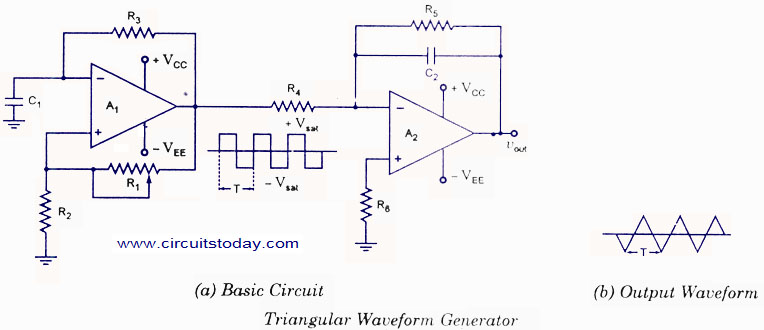
A triangular wave generator utilizing an operational amplifier (op-amp) is presented. The theoretical foundation and operation of the circuit diagram are discussed. The integration of a square wave signal results in the generation of a triangular wave. A practical...
Circle i represents a two-phase grid connection line for an AC technology turbine shed, which consists of two lines. A voltage is generated between Ri through a Buck converter, with components R1 and R3 dividing the output. The sampled...
An operational amplifier (op amp) configured as a comparator generates a 10-V peak-to-peak square wave output with a 100-mV input signal at a frequency of up to 15 kHz. The resistor R5 can be adjusted to achieve symmetry in...