
Linearized platinum resistance thermometer

The described circuit utilizes the LT-1001 precision operational amplifier, which is known for its low input offset voltage and minimal drift with temperature variations. This makes it suitable for applications requiring high accuracy in temperature measurement. The calibration process at the wafer level ensures that the device is optimized for performance before it is integrated into the final application.
When adjustments to the input offset voltage are needed, the nulling circuit (Figure 10-4B) can be employed. This circuit is designed to provide a means of fine-tuning the offset without introducing additional drift, thereby maintaining the circuit's overall accuracy. The null range of approximately ±100 V indicates that significant adjustments can be made to accommodate variations in system requirements or component tolerances.
In practice, the implementation of this circuit involves careful consideration of the surrounding components, including resistors and capacitors that may be used in conjunction with the LT-1001. Proper layout and thermal management are essential to maintain accuracy and reliability, especially in environments where temperature fluctuations are expected. The circuit's design should also take into account power supply decoupling to minimize noise and improve performance.
Overall, this precision temperature measurement circuit exemplifies the integration of advanced electronic components to achieve high levels of accuracy and stability, making it suitable for a wide range of applications in industrial, medical, and scientific fields.With the values shown, this circuit has a ±0. 025 °C accuracy over 0 ° to 100 °C. The input offset voltage of the LT-1001, and its drift with temperature, are permanently trimmed at wafer test to a low level. However, if further adjustment of VOS is necessary, nulling with the circuit of Fig. 10-4B will not degrade drift with temperature. The Fig. 10-4B offset circuit has an approximate null range of ±100 V. o Raytheon U near Integrated a rcuts 1989, p. 4-45. 🔗 External reference
Related Circuits
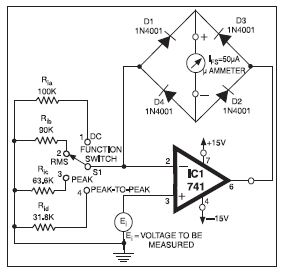
The full-scale deflection of the universal high-input-resistance voltmeter circuit depends on the position of the function switch. The term IFS in the equations refers to the meter's full-scale deflection current rating in amperes. It is important to note that...
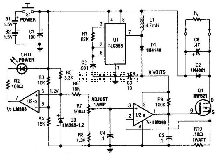
Useful for low-resistance measurements, this 1-A current source will produce 1 A in unknown resistance Rx. For best results, Rc should be less than 1 to 2, because only 3 V are available. Ul is a flyback converter to...
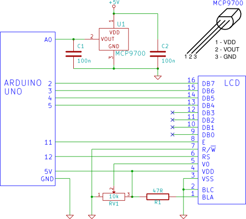
A temperature sensor (MCP9700 linear active thermistor IC) and LCD are connected to the Arduino in this tutorial. The Arduino reads the temperature from the MCP9700 on analog pin A0 and displays the temperature on the LCD. The circuit involves...
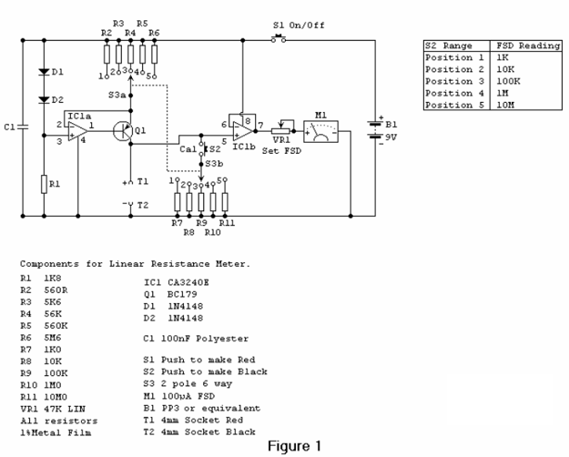
Most analog multimeters are capable of measuring resistance over a wide range of values, but they can be inconvenient to use due to the reverse reading scale, which is also non-linear. Analog multimeters, often referred to as VOMs (Volt-Ohm-Milliammeter), are...
A digital thermometer is being planned for construction using an ATmega8 microcontroller and an LM335 temperature sensor. Guidance is sought on how to proceed with the project, particularly concerning the display components. The digital thermometer circuit utilizes the ATmega8 microcontroller,...
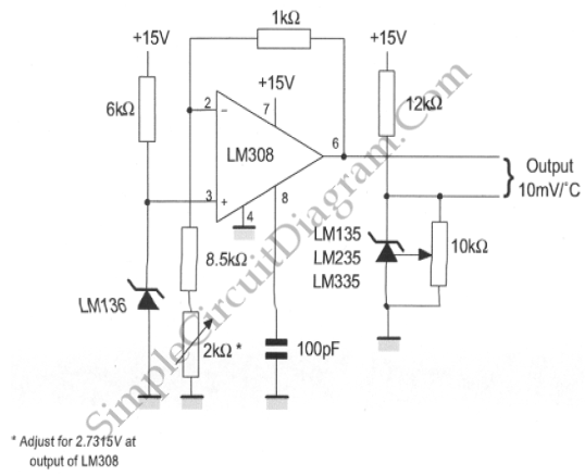
The LM135/235/335 temperature sensor is designed for ease of absolute temperature reading, providing all positive values for any frequency. This is why a voltage of 2.7315V is observed at 0 degrees. The LM135/235/335 series of temperature sensors are precision devices...