
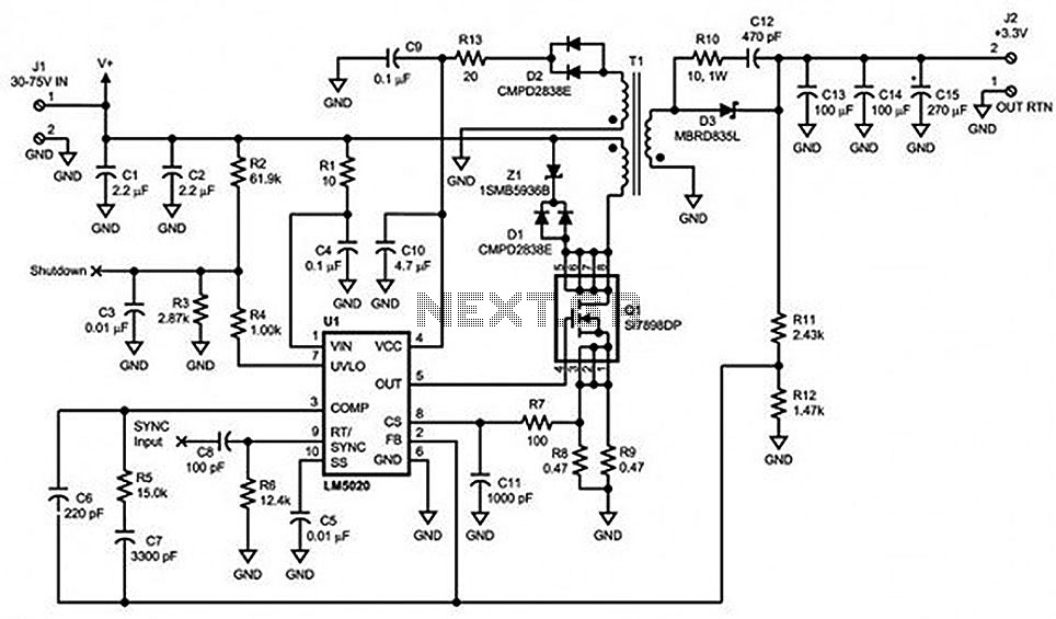
LM5020 High Voltage - Speed PWM Controller
The LM5020 is a versatile integrated circuit designed for use in power supply applications. It incorporates various features that enhance its performance and reliability.
The connection diagram of the LM5020 illustrates how the device interfaces with other components in a power supply circuit. It typically includes input and output pins, control pins for enabling or disabling the device, and feedback pins for voltage regulation. Understanding the pin descriptions is crucial for proper circuit design, as each pin has a specific function that contributes to the overall operation of the device.
The functional block diagram provides a high-level view of the internal architecture of the LM5020. It shows the arrangement of key components such as the internal high-gain error amplifier, which is responsible for maintaining output voltage stability by comparing the feedback voltage to a reference voltage. The error amplifier adjusts the duty cycle of the switching transistor to regulate the output voltage effectively.
The line under voltage lockout (UVLO) circuit is a protective feature that prevents the LM5020 from operating under low input voltage conditions, which could lead to unstable performance or damage. This circuit monitors the input voltage and disables the device if it falls below a predetermined threshold, ensuring safe operation.
The cycle-by-cycle overcurrent protection function is another critical feature of the LM5020. This mechanism detects overcurrent conditions in real-time and limits the output current by adjusting the duty cycle of the switching signal. This protection helps prevent overheating and damage to the power supply and connected components.
The oscillator frequency of the LM5020 is adjustable, allowing designers to optimize the switching frequency for their specific application. This flexibility can improve efficiency, reduce electromagnetic interference (EMI), and enhance overall performance.
Lastly, the duty cycle limit options provide additional control over the maximum duty cycle of the switching signal. This feature is essential for ensuring that the power supply operates within safe limits, particularly in applications where load conditions may vary significantly.
In summary, the LM5020 integrates multiple functionalities that make it suitable for various power supply designs, with essential features such as voltage regulation, protection mechanisms, and frequency adjustment capabilities. Understanding these elements is crucial for effective implementation in electronic circuits.find sections such LM5020 Connection Diagram and pin descriptions, the functional block diagram of the device, line Under Voltage Lock Out (UVLO) circuit, an internal high gain error amplifier, a cycle-by-cycle over current protection function, sets the LM5020 oscillator frequency, and The LM5020 duty cycle limit options 🔗 External reference
Related Circuits
The SA9614 is an RF amplifier utilized for signal conversion and automatic laser power control (ALPC) between the CD optical pickup head and the decoding chip. The SA9614 incorporates an interface for the CD optical diode RF signal amplifier...
High voltage electrolytic capacitors in valve equipment can deteriorate if the equipment is unused for an extended period. This deterioration manifests as reduced capacitance and significantly increased leakage current. In some instances, the capacitor may become nearly short-circuited. Using...
The circuit utilizes a Zener diode D1 to limit surge voltage and incorporates a four-diode rectifier bridge to prevent reverse voltage. The Zener diode D1 is rated at 36V, with optional choices being 1N4753A or 6KE39A. When the loop...
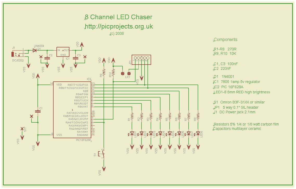
This compact circuit operates 8 LEDs directly driven from a PIC microcontroller, accompanied by a single mode control switch. The firmware controls the LEDs using a 5-bit PWM signal, enabling four levels of intensity for each LED channel: off,...
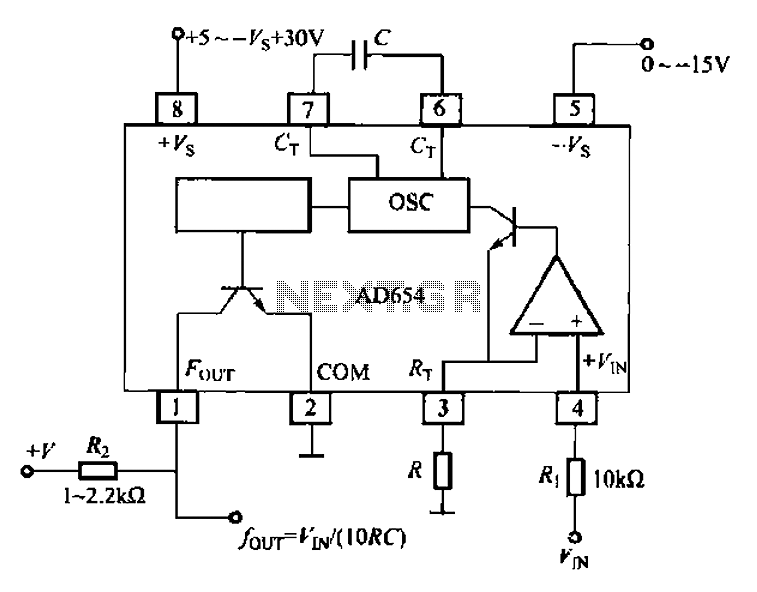
The AD654 voltage-frequency converter is a low-cost device that operates with a single supply voltage ranging from +5V to +36V, as well as with dual supplies of +5V to +18V. It can handle a maximum input voltage of 36V...
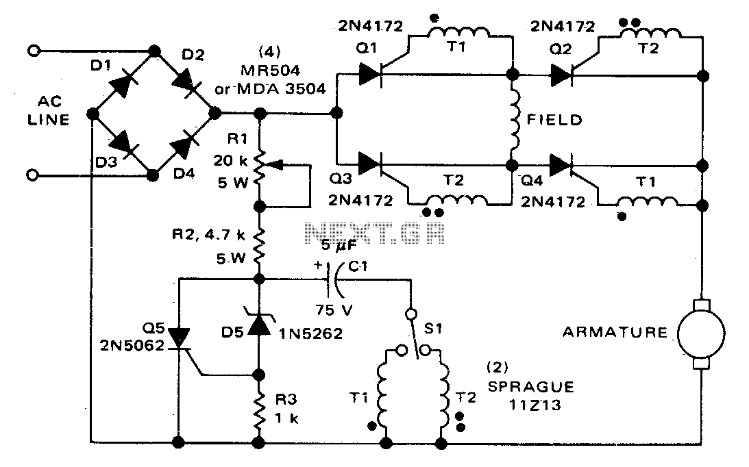
The circuit can control the speed and direction of rotation of a series-wound DC motor. Silicon controlled rectifiers Q1-Q4 are arranged in a bridge configuration and are triggered in diagonal pairs. The selection of which pair to activate is...