
Logic Probe Project

Resistor specifications include R1, R2, R8, and R9 at 3.3 MΩ (orange, orange, green), R3 and R5 at 33 kΩ (orange, orange, orange), R4 at 47 kΩ (yellow, violet, orange), R6, R7, and R10 at 820 Ω (gray, red, brown), and R11 at 2.2 MΩ (red, red, green). Capacitor C1 is 1 nF (103Z) ceramic, while C2 is a 100 nF poly film (DT98G). The semiconductors include IC1 (CA3240E, recommended replacement: LM393N voltage comparator) and IC2 (555 timer, recommended replacement: NE555N). The logic probe utilizes a common cathode two-color LED and features a rectangular shape for the green LED. Miscellaneous components include wire links (LK1-7) and gold crocodile clips (CN1 for red and CN2 for black). The probe tip can be constructed from a long M3 bolt, and the assembly is housed in a compact case, facilitating handheld operation. The circuit connections are made easy with approximately half-meter-long supply leads terminated in color-coded crocodile clips for clear identification. The Veroboard layout for the CMOS Logic Probe is designed for a board with 12 copper strips and 26 holes, ensuring straightforward construction while adhering to proper handling precautions for the MOS device used in the circuit.CMOS logic integrated circuits are extremely versatile devices which are used a great deal in modern electronic circuits. Like any logic circuits, those which employ CMOS devices can be difficult to test using an ordinary multi-meter as both static and pulsing voltages are involved.
A voltage reading of half the supply potential could be a static voltage and indicative of a fault, or it could be produced by a high frequency squarewave signal giving an average voltage of half the supply voltage with no fault present in this part of the circuit. Ideally an oscilloscope should be used for testing this type of equipment, but where this is not possible for some reason a logic probe makes an excellent alternative.
This simple logic probe is intended for use with CMOS logic circuits, is powered from the circuit under investigation, and has a current consumption of only around 0 to 20mA (depending on the supply voltage and logic state indicated by the probe). The logic state detected by the unit is indicated by a two-LED display: one of the display LEDs IS a multicolour type and the other is an ordinary green type.
The following table shows the display obtained from various input signal conditions. When the input is pulsing at high speed it is possible that D1 will be red or green instead of yellow, and this simply indicates that the mark-space-ratio of the input signal is far from being one-to-one. D1 will be red if the input is high for the majority of the time, or green if it is predominantly low.
If the input is pulsing slowly, unless the pulses are extremely brief, D1 will be seen to switch from red to green and so on in sympathy with the input signal. Separate stages are used to drive the two indicator LEDs, a dual operational amplifier being used to drive D1 and a 555 monostable driving D2.
Figure 1 shows the circuit diagram of the CMOS Logic Probe. Both sections of IC1 are used as voltage comparators rather than operational amplifiers, and these each have one input connected to a reference voltage, and the other taken to the input of the probe. The unit must indicate a high input state if the input voltage is more than about 70% of the supply voltage, and allow input state if the input is at less than about 30% of the supply potential.
R3 to R5 form a potential divider which gives reference voltages of approximately 30% and 70% of the supply voltage. If the input is low, IC1a`s non-inverting input will be at a higher potential than the inverting input so that the output goes high and switches on D1b.
IC1b has the opposite input states so that its output goes low and D1a is switched off. This gives a green indication from D1. With the input in the high state IC1a`s inverting input is taken to a higher voltage than the non-inverting input, causing the output to go low and switch off D1b. IC1b`s non-inverting input will now be at a higher voltage than the inverting input, causing IC1b`s output to go high and switch on D1a so that a red indication is obtained from D1.
If the input is between the two logic states the outputs of the two comparators will both assume the high state so that the red and green sections of D1 switch on to produce a yellow display. R1 and R2 bias the input between the two logic levels so that the unit will indicate a fault condition (with D1 in the yellow state) if the input is taken to an open circuit test point.
This section of the circuit does not enable the user to differentiate between a static level between the two logic states and a high frequency pulse signal, since the latter will cause both sections of D1 to switch on in turn and give the impression of a yellow display due to the switching action being too fast to be seen. This is overcome by applying the input signal to the trigger input of a 555 monostable. Normally R8 and R9 hold the input of IC2 above the trigger threshold, but if there IS a pulsing input signal it will be coupled to the input of IC2 by C1 and on negative transistions IC2 will be activated.
LED indicator D2 is then switched on for about 0. 25 seconds each time IC2 is triggered, but with a high frequency input signal the circuit will be retriggered almost as soon as each output pulse ceases, and D2 will appear to light continuously. C1 blocks steady state inputs so that IC2 is not triggered, except possibly for a single triggering when the input is taken to a new logic state, with a consequent brief flash from D2.
Resistors - ALL Min Res R1, 2, 8, 9 3M3 (Orange Orange Green) 4 off (M3M3) - 13p R3, 5 33k (Orange Orange Orange) 2 off (M33K) - 9p R4 47k (Yellow Violet Orange) (M47K) - 9p R6, 7, 10 820W (Grey Red Brown) 3 off (M820R) - 9p R11 2M2 (Red Red Green) (M2M2) - 13p Colour Code Convertor PC Windows Programme. Very good and easy to us. I recommend it! Capacitors C1 1 nF (103Z) Ceramic 1 (Discontinued) All ceramics are measured in pico farads. So 104 = 10, 000 pico farads = 10 nano farads. See Engineering Notations for description of measurements. C2 100n Poly Film (DT98G) - 10p Semiconductors IC1 CA3240E - Use LM393N Voltage Comparator (Discontinued) - Was £1.
38 IC2 555 Timer - NE555N - replacement for ICM7555 (GH66W) - 37p D1 Common cathode 2 colour LED (Discontinued) D2 [Rectangular] Shape LED R1 Green (YY46A) - 16p Miscellaneous LK1-7 Wire links between circuit tracks. CN1 Gold Croc Clip Red (FS53J) - 52p CN2 Gold Croc Clip Black (FS55K) - 52p One Meter of 2-way Cable for power lead.
Logic Probe Tip - Long M3 bolt Small moulded black plastic case (FT31) - 99p 124mm long by 33mm wide by 30mm deep Vero-board, 81 x 14 holes - Stripboard (FL17T) - £4. 99 All components available from Maplin Electronics on-line (through the Post or from there 40 UK Shops).
The Logic Probe project was published in the Maplin Magazine. Maplin Electronics - postal retailer with shops of 12, 000 quality Electronic Components and Items, large stock, own catalogue. P&P £2. 50, free over £35 incl. VAT. The Veroboard layout for the CMOS Logic Probe is shown In Figure 2 and this is based on a board having 12 copper strips by 26 holes.
Construction of the board is quite straightforward apart from the fact that IC1 is a MOS device, and the normal MOS handling precautions must be taken with this device. IC2 is a CMOS device but due to its internal protection circuitry it does not require any handling precautions.
In use the unit will probably be most convenient if it is fitted in a small case that can be comfortably hand-held. Thee probe tip, which can simply consist of a long M3 bolt, is fitted at the front end of the case and the two display LEDs are mounted off-board at the rear end of the case.
The case is drilled to take the two supply leads, and these are about half a metre long and terminated in crocodile clips to permit easy connection to the circuit under test. The crocodile clips are different colours (red for the positive lead and black for the negative one) so that the two leads are easily identified.
🔗 External reference
Related Circuits
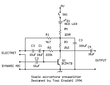
This is a simple microphone preamplifier circuit designed for use between a microphone and a stereo amplifier. This circuit is compatible with standard home stereo amplifier line, CD, aux, and tape inputs. It can accept both dynamic and electret...
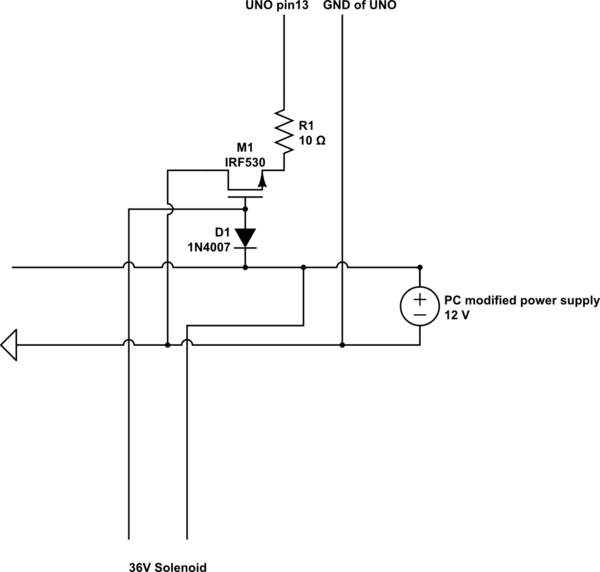
A 9 V DC battery initially powered the solenoid valve effectively. However, the solenoid did not generate sufficient force due to inadequate DC power. A modification was made to use a computer power supply as the power source. Providing...
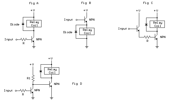
The schematic below illustrates four methods of controlling a relay with a digital logic signal. Figure A can be used in most cases where the relay coil requires 100 mA or less and the input current is 2 milliamps...
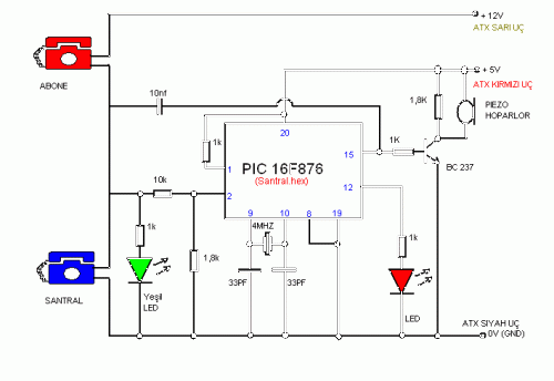
This simple telephone switching system is designed by Dr. Mustafa Kemal Peker for training purposes. All responsibility belongs to the user. Schematic and circuit details are included. The telephone switching system designed for training purposes serves as an educational tool...
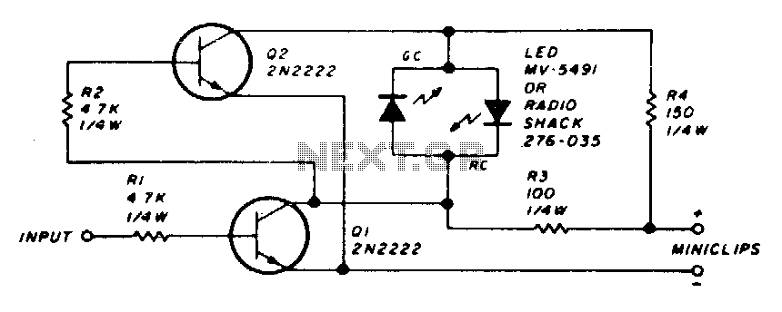
The circuit employs a dual LED configuration. When power is supplied to the probe through the power leads, and the input is connected to a low level or ground, transistor Q1 is turned off. This results in transistor Q2...
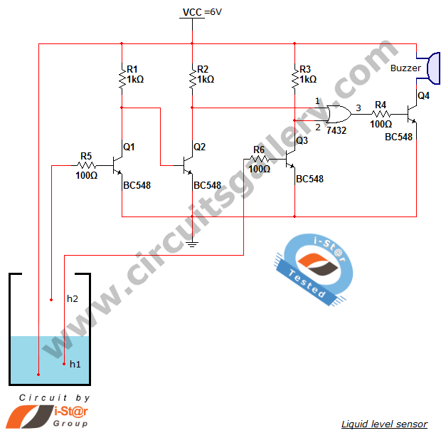
A variety of small electronic projects related to water level sensors have been posted in the Circuits Gallery. This particular project is designed for school students to detect the water level within a water tank or any other water...