
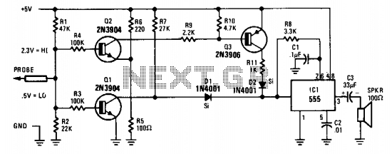
Logic probe yields three discrete states

The described circuit functions as a logic probe, utilizing a dual LED to visually indicate the status of a digital signal. The design incorporates two NPN transistors, Q1 and Q2, which operate in a complementary manner. When the probe's input is at a low logic level (ground), Q1 is non-conductive, effectively cutting off its current flow. This lack of current through Q1 allows Q2 to become active, as the positive voltage at its base enables it to conduct. The conduction of Q2 leads to the forward biasing of the green LED, signaling a low logic state.
In contrast, when the probe is applied to a high logic level, Q1 becomes conductive, allowing current to flow through it while simultaneously turning off Q2. This complementary operation results in the red LED being forward-biased, indicating a high logic state.
The circuit also accommodates alternating signals, which can occur in digital applications. When an alternating signal is applied, both transistors will switch on and off in rapid succession. This rapid alternation causes the red and green LEDs to light up in a manner that blends their colors, producing an amber output. This feature is particularly useful for identifying not only static logic levels but also dynamic signal changes, making the probe versatile for troubleshooting and testing digital circuits.
The overall design emphasizes simplicity and effectiveness, providing clear visual feedback through the dual LED arrangement. The use of transistors allows for quick response times, making it suitable for real-time analysis of digital signals. The logic probe can be an essential tool in electronics for engineers and technicians, aiding in the diagnosis and verification of circuit behavior.The circuit uses a dual LED. When power is applied to the probe throughthe power leads, and the input is touched to a low level or ground, Ql is cut off. This will cause Q2 to conduct since the base is positive with respect to the emitter. With Ql cut off and Q2 conducting, the green diode of the dual LED will be forward biased, yielding a green output.
Touching the probe tip to a high level will cause Ql and Q2 to complement, and the red diode will be forward biased, yielding a red output from the LED An alternating signal will cause alternating conduction of the red and green diodes and will yield an indication approximately amber. In this manner, both static and dynamic signals can be traced with the logic probe.
Related Circuits
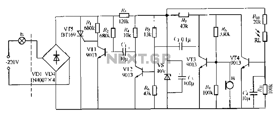
This circuit describes a sound and light control delay system for a walkway stairs light switch. It involves various components including 220V AC electric bulbs, diodes (VD1-VD4), and resistors. The circuit utilizes a rectifier regulator to stabilize the voltage...
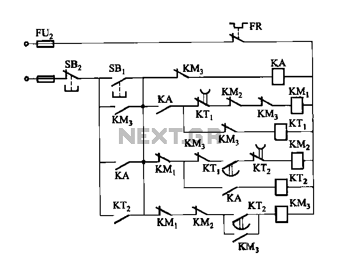
Figure 3-118 illustrates an automatic acceleration control circuit. This circuit employs a male contactor time relay, enabling the motor to start automatically at a low speed before transitioning to high-speed operation. The automatic acceleration control circuit depicted in Figure 3-118...
After the battery is connected, the movement of the touch stick activates the light source, which illuminates the photosensitive tube and generates a light current. This triggers the first level 3DG6 to turn on, allowing the emitter to output...
The probe's input circuit detects the signal condition and generates a low-pitched tone for low-level signals (below 0.8 V) or a high-pitched tone for high-level signals (above 2 V). The tone probe employs sound to indicate the status of...
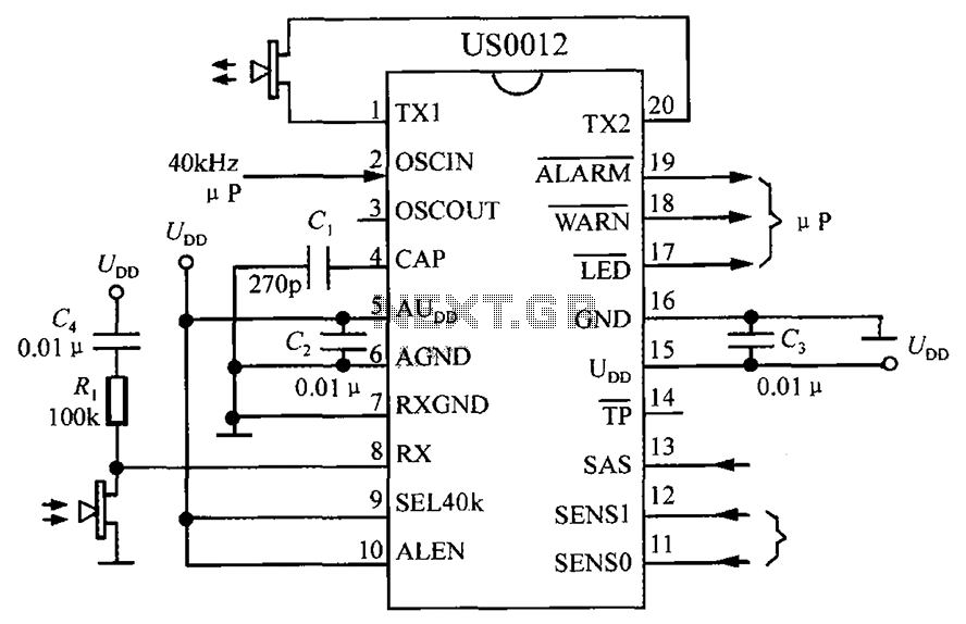
The circuit consists of the US0012 ultrasonic interference detection system, as illustrated in the accompanying figure. When the SEL40k termination is set to high, it selects a clock frequency of 40kHz. The US0012 module can perform several tasks: it...
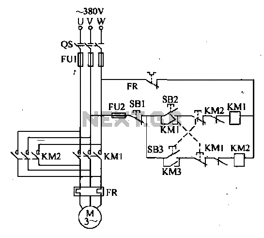
The forward and reverse dual interlock control circuit is based on the control circuit depicted in Figure 4-4, with an enhancement that incorporates a composite mechanical button interlock. The advantage of this circuit is that it allows the motor...