
long delay timer schematics
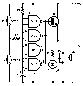
The described timer circuit is a practical solution for managing power consumption in portable radio devices, particularly beneficial for users who may fall asleep while listening. The design employs a simple RC time constant created by R1 and C1, which directly influences the duration before the radio switches off. The choice of a 4011 Quad 2 Input NAND Gate for IC1 is notable, as it allows for the parallel configuration of multiple gates, enhancing the reliability of the circuit's operation.
The momentary switch P2 serves as the activation point, and its design ensures that the circuit remains in a low-power state until engaged. The charging and discharging behavior of C1, in conjunction with R1, establishes a predictable timing mechanism. This feature is crucial for applications where precise timing is necessary, such as in scenarios where users may not be able to manually switch off the device.
Transistor Q1 plays a critical role in driving the load, with its emitter providing a direct connection to the device. The capability to connect a relay expands the circuit’s functionality, enabling it to control devices with higher power requirements. This versatility makes the timer suitable for a wide range of applications beyond just portable radios.
Overall, the circuit's design allows for easy adjustments to the timing interval, making it adaptable to different user needs. The inclusion of P1 for manual interruption of the timer adds an additional layer of control, ensuring that users can override the automatic shut-off feature if desired. The schematic design is straightforward, making it accessible for hobbyists and engineers alike, while also providing a robust solution for energy management in portable electronics.This timer was designed mainly to switch off a portable radio after some time: in this way, one can fall asleep on the sand or on a hammock, resting assured that the receiver will switch off automatically after some time, saving battery costs. R1 and C1 provide a very long time constant. When P2 is momentarily closed, C1 discharges and the near ze ro voltage at its positive lead is applied to the high impedance inputs of the four gates of IC1 wired in parallel. The four paralleled gate outputs of the IC go therefore to the high state and the battery voltage is available at Q1 Emitter.
When P2 is released, C1 starts charging slowly through R1 and when the voltage at its positive lead has reached about half the battery voltage, the IC gate outputs fall to zero, stopping Q1. This transistor can directly drive a portable radio receiver or different devices drawing a current up to about 250mA.
Connecting a Relay across the Emitter of Q1 and negative ground, devices requiring much higher voltage and current operation can be driven through its contacts. Pushing on P2 for 1 to 5 seconds, the circuit starts and then will switch off after about 35 minutes.
This time delay can be varied by changing R1 and/or C1 values. P1 will stop the timer if required. A 4011 Quad 2 Input NAND Gate was used for IC1, but many other CMos gates or inverter arrays can be used in its place, e. g. 4001, 4002, 4025, 4012, 4023, 4049, 4069. With these devices, all inputs must be tied together and also all outputs, as shown in the Circuit diagram.
🔗 External reference
Related Circuits
For many applications, it is necessary to delay signals. Consider applications in automation and control systems. A signal delay circuit can be established using two monoflops. Signal delay circuits play a crucial role in various electronic applications, particularly in automation...
Ensure that connections are verified against the circuit diagram and schematic provided below. This can be utilized while following the tutorial video. The circuit diagram serves as a crucial reference for accurately assembling electronic components in a project. It illustrates...
This circuit was developed in response to requests from website visitors for a timer that can emit a beep after intervals of one, two, three minutes, and so forth, for jogging purposes. As depicted in the circuit diagram, SW1...
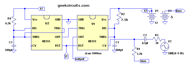
This text continues the discussion on a Class D amplifier utilizing a 555 timer chip. In reviewing previous schematics, the inclusion of a second 555 timer (U2) raises questions. The primary function of U2 is to provide a constant...
This timer was designed for people wanting to get tanned but at the same time wishing to avoid an excessive exposure to sunlight. A Rotary Switch sets the timer according to six classified Photo-types. A Photo resistor extends the...
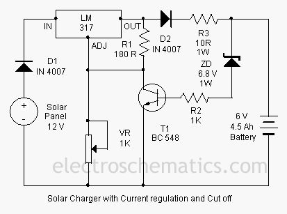
This is a solar charger circuit designed to charge Lead Acid or Ni-Cd batteries utilizing solar energy. The circuit captures solar energy to charge a 6-volt, 4.5 Ah rechargeable battery for various applications. It includes voltage and current regulation,...