
Class D amp made easy with 555 timer IC
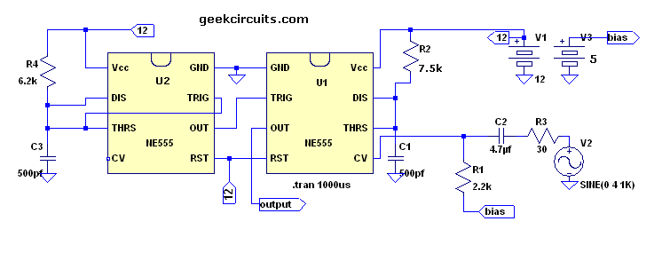
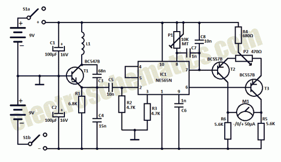
The Class D amplifier circuit described employs a 555 timer IC as the core component for generating the necessary PWM signal. The circuit utilizes two 555 timer chips, where U1 is the primary timer generating the PWM signal and U2 serves the role of maintaining a stable frequency trigger for U1. This design choice is critical for ensuring that the PWM carrier frequency remains consistent, particularly during audio modulation.
The feedback mechanism is established by connecting the output of U1 (pin 3) back to the RC timing network at pins 6 and 2. This configuration allows the circuit to operate in an astable mode, achieving a duty cycle of 50%. The astable operation is essential for effective PWM generation, which is crucial for driving the output stage of the Class D amplifier. The audio signal is applied to pin 5 of U1; however, care must be taken as distortion may occur at higher modulation levels, particularly when using the circuit at lower volume settings.
The implementation of negative feedback through a 2N3904 transistor is a notable enhancement to the circuit. This transistor allows for self-biasing of the amplifier, which can significantly improve audio fidelity by stabilizing the operating point of the output stage. It is important to consider the variations in the hFE of the 2N3904, as these can lead to differences in sound quality. For applications requiring greater consistency, the use of an operational amplifier may be advisable.
The unexpected audio quality resulting from the self-oscillating nature of the circuit presents an intriguing characteristic, as it combines both PWM and FM modulation effects. This phenomenon may provide insights into the advantages of self-oscillating Class D amplifier designs, which are often favored in high-fidelity audio applications. Future designs and modifications to this circuit will explore additional enhancements and configurations to further optimize performance.This is a continuation of my previous article regarding class d amp using 555 timer chip. Looking back to several schematics on that article, some of you may wonder why I include another 555 as U2 in the drawing. The main purpose of this U2 is to establish constant frequency trigger on pin 2 of U1 in such a way of maintaining stable PWM carrier fr
equency during audio input modulation. By scrutinizing the behavior of the circuit in LT spice simulator, and listening to their sound thru the breadboard circuit layout, the sound is good and clean. Of course there are some interesting ways in doing this but the most interesting thing for me to satisfy my curiosity is to try to use U1 alone without the trigger U2 to conserve space and cost to the lowest value as possible.
In this case, by feeding back the output pin 3 to the RC time network on pin 6 & 2 the resulting switching mode is astable with 50% duty cycle. I tried to apply music to pin 5 as usual but noticed a distorting sound even at lower volume settings.
Fig. 1 Schematic of 555 circuit with negative FB added. Please take note that 2N3904 varies on their hfe depending on it`s production binning. So you may get different sound quality due to this variations. Better opt for opamp if you want. By implementing negative feedback thru the help of 2N3904 transistor to self bias it in a conventional way, (see fig. 1) the resulting sound was so good that it seems better than the sound produced by using 2 chips. Why Well, I don`t have specific answer for this question at the moment and by observing the behavior of the waveforms while the circuit is being modulated reveals a mixture of PWM and FM at the same time.
It is quite surprising for me to hear a music in class d amp having a mixture of PWM with FM owing to the fact that most of my class d design works are always time based as opposed to self oscillating approach. I think class d amp design based in self oscillating mode experience the same thing like this which makes it (self oscillating) more favored my most audiophiles.
More circuits to follow. 🔗 External reference
Related Circuits
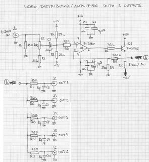
The circuit presented here has numerous applications. Essentially, the distribution amplifier receives a composite video signal from a video player (VCR) or a video generator (analog output) and buffers it, allowing it to be simultaneously sent to up to...
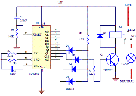
This electronic timer switch will turn on a light for 100 seconds, turn it off for another 100 seconds, and then turn it on again for 100 seconds after an hour of powering up the circuit. It is a...
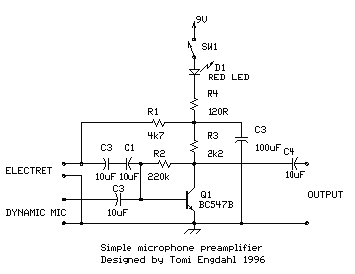
This is a simple microphone preamplifier circuit designed for use between a microphone and a stereo amplifier. This circuit is compatible with standard home stereo amplifier line, CD, aux, and tape inputs. It can accept both dynamic and electret...
Utilize this FM antenna amplifier in locations where the reception of FM stations is poor. This circuit is specifically designed for this purpose. The FM antenna amplifier circuit is engineered to enhance signal strength for FM radio stations, particularly in...
This homemade metal detector circuit is designed to locate objects made of materials with relatively high magnetic permeability. While it may not be sensitive enough for detecting buried coins, it can effectively identify larger metallic treasures. The circuit operates...
This FM booster allows for clear reception of programs from distant FM stations. The circuit features a common-emitter tuned RF preamplifier utilizing the VHF/UHF transistor 2SC2570 (only labeled as C2570 on the transistor body). The input coil L1 is...