
Long Delay TimerCircuit
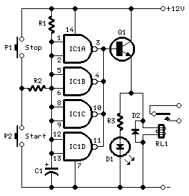
The timer circuit is an effective solution for automatic shut-off applications, particularly for battery-operated devices like portable radios. The design leverages the charging and discharging characteristics of the capacitor C1, combined with the resistive path provided by R1, to create a time delay that can be fine-tuned for specific needs. The use of a quad NAND gate IC allows for a compact arrangement of logic gates, which simplifies the circuit and reduces component count.
In operation, when P2 is pressed, the initial discharge of C1 ensures that the logic gates receive a low signal, prompting them to output a high signal that activates Q1. This transistor acts as a switch, allowing current to flow to the connected device, such as a radio. The gradual charging of C1 through R1 means that the voltage across C1 will rise slowly, providing a predictable time delay before the gates revert to a low state, which in turn turns off Q1.
The capability to control higher current devices through a relay adds versatility to the design. By incorporating a relay, the circuit can manage appliances that exceed the direct current rating of Q1, expanding the potential applications of the timer circuit. The adjustment of R1 and C1 values allows users to customize the shut-off time, making it suitable for various scenarios, from short naps to longer periods of inactivity.
The inclusion of a manual stop switch (P1) provides an additional layer of control, allowing the user to terminate the timer function at any point, enhancing the circuit's usability. Overall, this timer circuit exemplifies a practical and efficient approach to managing power consumption in portable electronic devices.This timer was designed mainly to switch off a portable radio after some time: in this way, one can fall asleep on the sand or on a hammock, resting assured that the receiver will switch off automatically after some time, saving battery costs. R1 and C1 provide a very long time constant. When P2 is momentarily closed, C1 discharges and the near ze ro voltage at its positive lead is applied to the high impedance inputs of the four gates of IC1 wired in parallel. The four paralleled gate outputs of the IC go therefore to the high state and the battery voltage is available at Q1 Emitter.
When P2 is released, C1 starts charging slowly through R1 and when the voltage at its positive lead has reached about half the battery voltage, the IC gate outputs fall to zero, stopping Q1. This transistor can directly drive a portable radio receiver or different devices drawing a current up to about 250mA.
Connecting a Relay across the Emitter of Q1 and negative ground, devices requiring much higher voltage and current operation can be driven through its contacts. Pushing on P2 for 1 to 5 seconds, the circuit starts and then will switch off after about 35 minutes.
This time delay can be varied by changing R1 and/or C1 values. P1 will stop the timer if required. A 4011 Quad 2 Input NAND Gate was used for IC1, but many other CMos gates or inverter arrays can be used in its place, e. g. 4001, 4002, 4025, 4012, 4023, 4049, 4069. With these devices, all inputs must be tied together and also all outputs, as shown in the Circuit diagram.
🔗 External reference
Related Circuits
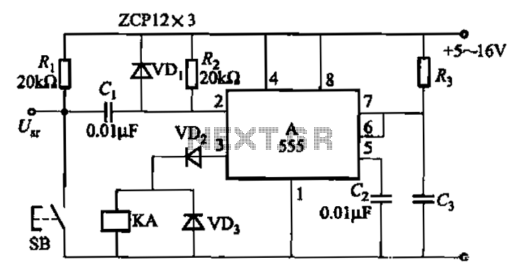
The 555 integrated circuit is utilized in a delay circuit configuration, functioning as a one-shot timer. The delay time can be adjusted using resistor R3 and capacitor C3. Typical values for R3 range from 1 kΩ to 10 MΩ,...
The CF5019 series are high-frequency, third overtone crystal oscillator module ICs. They integrate an oscillator circuit and an output buffer that function at high frequencies on a single chip. The oscillator circuit utilizes CMOS inverters and a built-in damping...
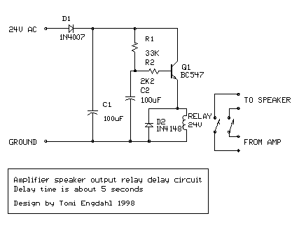
This circuit was designed for an audio amplifier project to control the speaker output relay. Its primary function is to manage the relay that activates the speaker output in the audio amplifier, ensuring a delay of approximately 5 seconds...
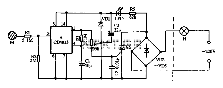
Diodes VD2 to VD5 and SCR form the main circuit of a touch switch. Resistor R5 and diode VD1 create a power supply circuit that outputs approximately 12V DC, which is utilized for a manifold A application. The circuit...
This circuit is a thyristor-based delay circuit known as a cut-off delay. It allows for a specified delay period after the thyristor is activated. The delay time of the circuit can be adjusted within 10 seconds by changing the...
Generating long delays of several hours can be achieved using a low-frequency oscillator and a binary counter. A single Schmitt Trigger inverter stage (1/6 of 74HC14) functions as a square wave oscillator, producing a low frequency of approximately 0.5...
Warning: include(partials/cookie-banner.php): Failed to open stream: Permission denied in /var/www/html/nextgr/view-circuit.php on line 713
Warning: include(): Failed opening 'partials/cookie-banner.php' for inclusion (include_path='.:/usr/share/php') in /var/www/html/nextgr/view-circuit.php on line 713