
Loudspeaking radio receiver with a bridge amplifier powered by free energy
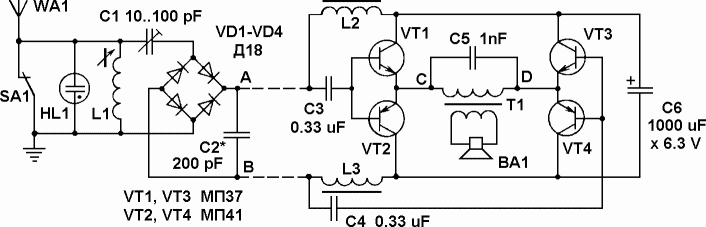
The schematic design described integrates a bridge detector circuit and a resonant tank, highlighting a compact and efficient configuration for audio amplification. The use of two wires for signal and power transmission simplifies the setup, enhancing usability in various applications. The automatic balancing of the amplifier arms is a notable feature, ensuring consistent performance without the need for a common wire. The choice of germanium transistors over silicon is critical due to their lower junction drop voltage, which minimizes crossover distortion in audio applications. The incorporation of a forward bias and high-frequency signal mixing techniques illustrates advanced methods for improving audio fidelity and amplifier efficiency. The design is particularly beneficial for low-power applications where simplicity and effectiveness are paramount. Overall, this circuit exemplifies innovative approaches to audio amplification, leveraging both traditional and modern techniques to enhance performance.While experimenting with different receivers and amplifiers powered by "free energy", it was found that it is more convenient to connect the audio amplifier to the receiver by using only two wires for audio signals and supply voltage. This would allow to use the radio receiver with no switches, just connecting headphones to the output of the recei
ver. The schematic diagram of the receiver is shown in Figure 1. From the detector bridge the circuit is completely symmetric, the detector is connected to the amplifier by two wires (the terminals A and B) and the output of the amplifier is connected to the loudspeaker (the terminals C and D) by two wires. The resonant circuit of the receiver comprised the antenna capacitance and inductance of the coil L1.
This solution provides a maximum power of the signal in the resonant tank circuit. The switch SA1 and the neon lamp HL1 are used to protect the receiver during thunderstorms. The static charge doesn`t build up in the antenna because the antenna connected to the ground through the coil L1. A bridge detector circuit (VD1 - VD4) is used in this receiver, it works very well for the inductive load.
The detector connected to the antenna through the capacitor C1, this capacitor is matching impedances between them. Once adjusted for maximum voltage across the amplifier, the capacitor C1 may be replaced with a constant capacitor with proper value.
The optimal capacitance of the capacitor C1 is about 47 pF for LW band. The output voltage of the detector is symmetric with respect to ground. Through the wires A and B the voltage passes from the detector to the input of the audio amplifier. At the input of the amplifier the voltage decomposes into AC and DC parts. The AC part feeds through the coupling capacitors C3 and C4 to the transistor bases of the bridge amplifier. The DC part charges through the low-frequency chokes the capacitor C6. The DC part is used for power supply. The receiver doesn`t have a common wire. The arms of the amplifier balances automatically, because the bases of the complementary transistors are connected together.
But transistors in this type of amplifiers don`t have a bias, they does not work in the class "B" but rather in the class "C". This leads to crossover distortion of the signal waveform, as shown in Figure 2(A). The graph shows the dependence of the output current in one arm of the amplifier (for example, VT1, VT2) on the input voltage.
We see a distorted output current for a sinusoidal input voltage. These distortions are especially noticeable with silicon transistors that have higher junction drop voltage of about 0. 5 V. Germanium transistors has lower junction drop voltage of about 0. 15 V, so they are used in the audio amplifier. Crossover distortion is related to the moments when voltage crosses zero point, that is very unpleasant to the ear.
Crossover distortions can be reduced by using a slight forward bias Ubias, as shown in Fig. 2(B). The distortions disappear but some initial current i0 appears, it makes the amplifier less efficient. The same result can be obtained by other means. If mixing the audio signal with a high frequency signal, as shown in Fig. 2(C). This method is used in tape recorders with AC bias, because the magnetization curve of the type is very similar to the amplifier transfer characteristic of a push-pull stage without bias.
By adjusting the amplitude of the "high frequency bias" the desired initial current (quiescent current) can be set, this current should not be too high, but sufficient to eliminate the distortion. But we already have high frequency bias, we got the detected RF voltage ripple. In the bridge detector circuit the ripple has twice the frequency of the carrier signal. We just need to tweak the value of the smoothing capacitor C2 (Fig. 1) to obtain the desired quiescent current. It`s better tweak the capacitor C2 when there is no audio transmission (bu 🔗 External reference
Related Circuits
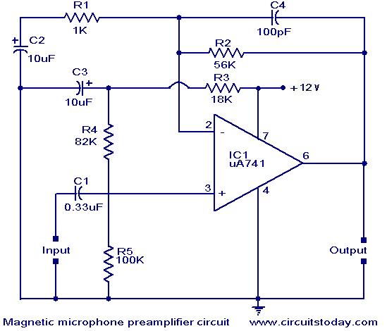
A preamplifier for magnetic pickups of record players is presented. The uA 741 is utilized as an AC-coupled non-inverting amplifier operating on a single supply. The amplifier gain is determined by the feedback components, where C2 manages the low-frequency...
I have attempted to create drivers for my H-bridge circuit using complementary emitters; however, the square wave outputs consistently run at a constant 25V instead of a ±10V square wave. The image is somewhat difficult to interpret, but it...
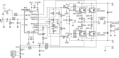
The following circuit illustrates the LME49810 integrated circuit used in a power amplifier circuit diagram. Features include improved drive capability for 4-ohm speaker impedance. The LME49810 is a high-performance audio power amplifier IC designed to deliver high output power with...
The NE5532 preamplifier is widely recognized for its excellent performance. It is now being utilized as a small power amplifier. While the general operational amplifier (op-amp) circuit remains similar, there are notable changes in some resistors and capacitors, leading...
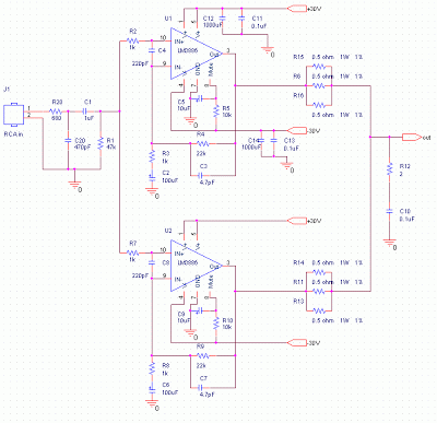
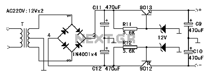
This audio amplifier design employs two LM3886 chips per channel in a parallel configuration, based on the PA100 parallel amplifier detailed in National Semiconductor's application note AN1192. It can deliver approximately 50W into an 8-ohm speaker and 100W into...

This circuit is a MOSFET power amplifier configured in an OCL (Output Capacitor-Less) topology. It delivers an output power of 100 watts and can utilize MOSFETs such as K134 and J49 or J162 and K1058. When driving an 8-ohm...
Warning: include(partials/cookie-banner.php): Failed to open stream: Permission denied in /var/www/html/nextgr/view-circuit.php on line 713
Warning: include(): Failed opening 'partials/cookie-banner.php' for inclusion (include_path='.:/usr/share/php') in /var/www/html/nextgr/view-circuit.php on line 713