
Low-Frequency Crystal Controlled Oscillator
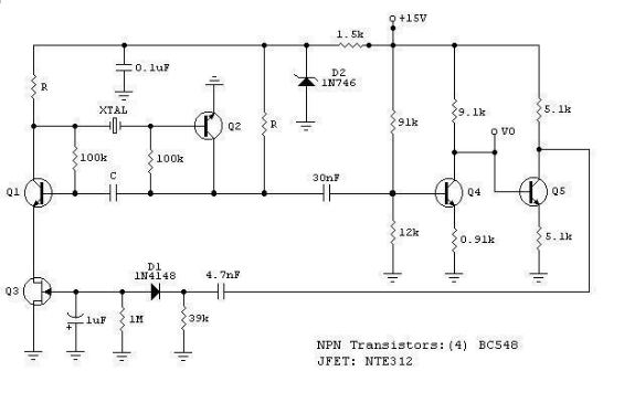
The described circuit functions as a precise low-frequency sine wave oscillator, ideal for testing low-frequency quartz crystal units. The design’s reliance on low-cost components, such as AF bipolar transistors and a JFET, makes it accessible for various applications. The automatic adjustment of the loop gain through Q3 ensures consistent performance across the specified frequency range while minimizing distortion. The isolation provided by Q4 and Q5 is crucial for maintaining signal integrity, preventing non-linear effects from impacting the output. The feedback mechanism established through the JFET enhances the circuit’s robustness against power supply variations, which is particularly beneficial in laboratory settings where environmental conditions may fluctuate. The ability to adapt the circuit parameters, such as the resistor values based on frequency, allows for fine-tuning according to specific operational requirements, making this design a reliable choice for RF engineers seeking to evaluate quartz crystal units effectively.The RF engineer sometimes has to look for an instrument that will check a low frequency quartz crystal unit reliably and rapidly. This is a difficult piece of equipment to find and the engineer often has to consult an electronic circuits handbook for the schematic of a circuit that will perform the task.
Unfortunately, there aren`t many such circu its in the technical literature currently available, and when found, they don`t always work as expected. A circuit that has been found to work at full satisfaction in the frequency range from 10 kHz to 500 kHz is illustrated in Figure 1.
This is a schematic of a low frequency sine wave oscillator featuring low distortion, wideband operation and crystal control. The circuit, originally developed for laboratory use, employs low cost AF bipolar transistors for the oscillator and amplifier sections and a JFET for loop-gain control.
Operation of the oscillator in the 10 kHz to 500 kHz frequency range has been found to be excellent, while measured distortion is kept under 0. 1 percent. Q1, Q2 and associated circuitry form a modified astable multivibrator in which the loop gain is automatically adjusted to the threshold of oscillation by means of field effect transistor Q3.
Q4 linearly amplifies the signal present at the collector of Q2 and isolates the oscillator section of the circuit from the output. This stage features wideband operation and delivers a clean 2. 5 Volt amplitude sine wave into a resistive load greater than or equal to 20 kohms. The stage comprising Q5 has a voltage gain of 1 and its sole purpose is to isolate the non-linear effects of rectifier D1 from the output.
Transistor Q4 also amplifies the minor changes in amplitude of the oscillator`s waveform due to temperature effects and/or power supply variations, so a magnified version of the perturbance is fedback to rectifier D1 producing a corresponding change in Q3`s gate voltage. This action modifies the FET`s drain-source resistance and hence adjusts the loop gain to a new value slightly above unity, just enough to maintain a constant amplitude in the output.
Figure 2 shows optimum values for capacitor C according to the crystal`s resonant frequency. Extra gain is needed from transistors Q1 and Q2 at frequencies below 40 kHz. This is due to the fact that low frequency crystals exhibit large values of series resistance, affecting loop gain (Table 1 compares typical values of series resistance for low frequency units). According to what has been stated, resistor R is made 10 kohms for frequencies under 40 kHz. Above this value, 1 kohm will do. 3) Due to the dynamic action of the JFET the output level is almost insensitive to power supply variations.
The 3. 3 Volt zener diode further enhances this result. 🔗 External reference
Related Circuits
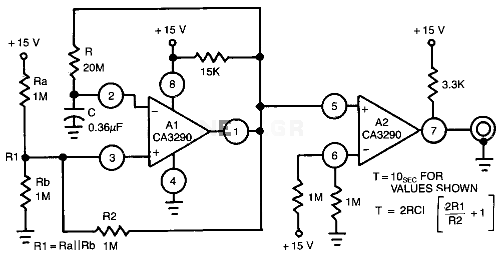
This circuit utilizes one half of the CA3290 BiMOS dual voltage comparator as a conventional multivibrator. The second half ensures frequency stability against the effects of output loading. Large values of the timing resistor, Rl, guarantee long time delays...
Millimeter-wave frequency bands are appealing due to their wide available bandwidths. Signals can be generated in various ways; however, for each type of oscillator, electronic tuning of the source in a defined and controlled manner is desirable. Employing a...
In a sine wave oscillator circuit, a thermistor and an incandescent lamp are often utilized to stabilize the output of the circuit at a fixed value. The resistance of... The sine wave oscillator circuit is designed to generate a continuous...
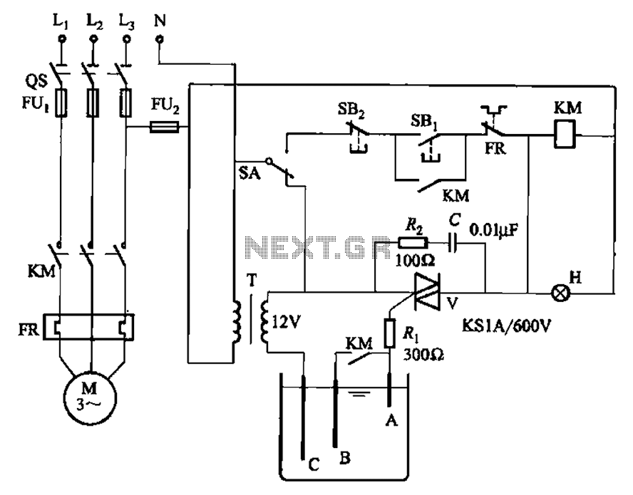
Bidirectional thyristor control manages the trigger voltage output from the step-down transformer at 12V when the water activates the electrodes. It is part of a drawable circuit that regulates the level. The circuit includes a current-limiting resistor (Ri) to...
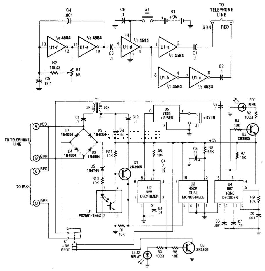
This system uses a transmitter operating at approximately 100 kHz to control a remote receiver. A line splitter can connect the transmitter to the active telephone line. The transmitter is a CMOS oscillator equipped with output buffer stages to...
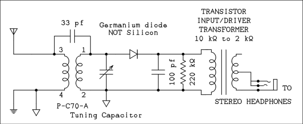
The P-C70-A from Antique Electronics Supply performs effectively, potentially even better than coils that can be wound manually. While winding coils can be an engaging experiment, an alternative circuit is available for those who prefer to bypass the winding...