
Low Voltage Preamplifier

This audio preamplifier circuit is designed for low-voltage applications, emphasizing performance in terms of gain, noise, and impedance characteristics. The architecture employs two bipolar junction transistors (BJTs) configured for optimal audio signal amplification. The emitter of T1 is set to approximately half the supply voltage to maximize the output voltage swing, which is critical for audio fidelity.
The direct coupling between T1 and T2 allows for efficient signal transfer while maintaining stability through closed-loop feedback. This feedback mechanism is essential for mitigating variations in temperature that could otherwise impact performance. T2 is responsible for achieving the desired voltage gain, and its collector current is optimized at 70 µA to minimize noise, a crucial factor in audio applications.
T1 operates as an emitter follower, which not only buffers the signal from T2 but also contributes to a low output impedance, measured at approximately 66 ohms. This low output impedance is advantageous for driving subsequent stages, such as power amplifiers, ensuring that the preamp can effectively interface with various loads without significant signal degradation.
Capacitor C3 plays a vital role in the circuit by decoupling the emitter resistor of T2. This decoupling affects the gain characteristics; without C3, the gain would be limited to the ratio of resistors R1 to R4. However, with C3 in place, the gain is influenced by the parallel combination of R4 and the input impedance of T1, as well as the small-signal emitter resistance of T2, resulting in a total gain of approximately 28 times.
The audio quality is also assessed through harmonic distortion measurements, which are reported at around 8%. While this level of distortion is acceptable for many applications, it indicates that careful design considerations were made to balance gain and fidelity.
One of the circuit's limitations is its relatively low input impedance, which can be attributed to the characteristics of T2 and the decoupling action of C3. To address this, resistor R7 is introduced in series with the base of T2, providing a slight increase in input impedance, which can enhance compatibility with various audio sources.
Overall, this low-voltage audio preamplifier circuit exemplifies a thoughtful design that prioritizes gain, noise performance, and impedance matching, making it suitable for integration into larger audio systems. It is a crucial component in the signal chain, ensuring that audio signals are amplified effectively before being sent to power amplification stages.This is a special low voltage version of my audio preamp. T1`s emitter voltage is biased close to half supply voltage (1. 5V) to allow for maximum output voltage swing. Both transistors are direct coupled and have closed loop feedback to aid temperature stability. T2 realizes the amplifiers full voltage gain, and for low noise operation, T2 collect or current is about 70uA. T1 merely buffers T2 and operates in emitter follower mode providing a good low output impedance. The overall S/N ratio measured at the output is shown below: Capacitor C3 decouples the emitter resistor of T2. Without C3 the gain of T2 would be approximately R1 / R4. With C3 the gain of T2 is now R4 in parallel with the input impedance of T1 / the small signal emitter resistance of T2.
The overall voltage gain of the circuit is around 28 times as shown below. Harmonic distortion is about 8%. One drawback of this circuit is that the input impedance is fairly low. This is because the input of T2 is low and has C3 decoupling the emitter. The inclusion of R7 in series with the base of T2 raises input impedance slightly. A plot of input impedance versus freqency response is shown below. The output impedance is very low, around 66 ohms as shown in the plot below. Note that this is a preamp and therefore designed to feed into a power amplifier not drive direct loads directly. 🔗 External reference
Related Circuits
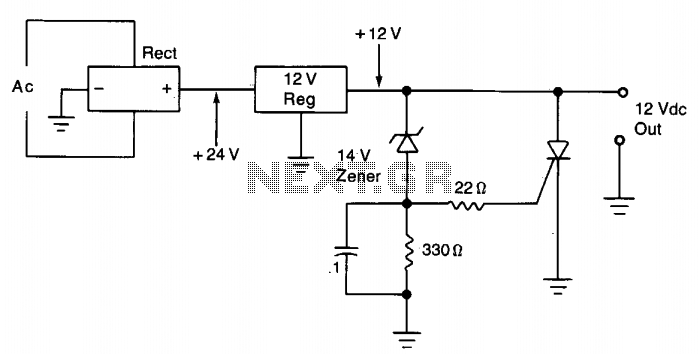
The silicon controlled rectifier (SCR) is designed to handle at least the current provided by the power supply. It is connected in parallel across the 12 V DC output lines but remains inactive until a voltage is applied to...
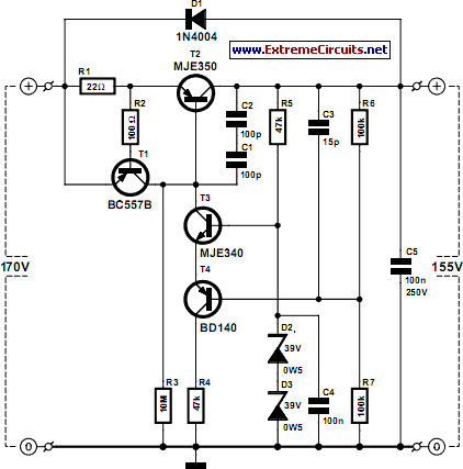
There are numerous circuits designed for low voltage regulators. However, for higher voltages, such as those required for valve circuits, the approach differs. This is the reason for the design of a simple regulator capable of handling these voltages....
The DS2422 temperature and data logger integrates the essential functions of a comprehensive data logger into a single chip. It features a temperature sensor, a real-time clock (RTC), memory, a 1-Wire interface, and a serial interface for an analog-to-digital...
2W resistors can be used with metal or carbon film resistors and optional paper capacitors, polypropylene capacitors, rated for 400V. A selection of different media is available in various configurations. Although there is no established polarity for vintage paper...
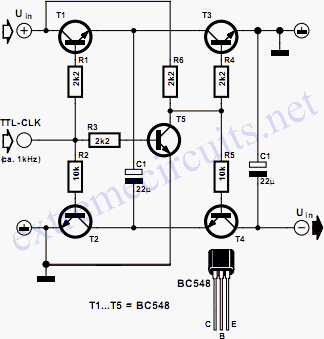
The circuit illustrated in the diagram allows for the generation of a negative voltage without utilizing integrated circuits. It employs five n-p-n transistors controlled by a TTL clock operating at approximately 1 kHz. When the clock signal is high,...
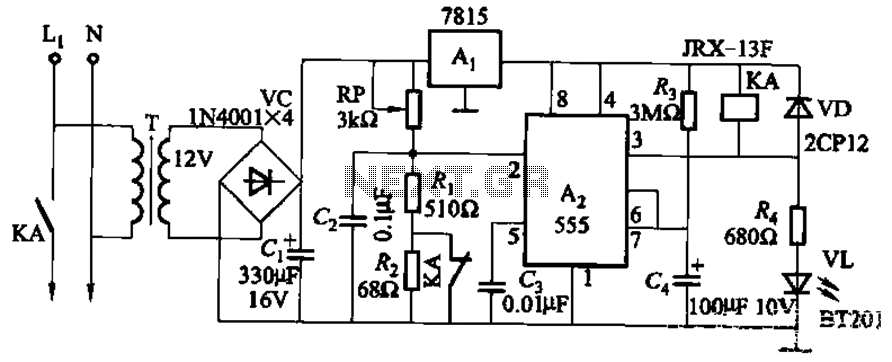
This circuit is applicable in refrigerators and other protective devices. It employs a 7815 three-terminal voltage regulator integrated circuit and an NE555 timer IC configured as a one-shot circuit for delay control. When the voltage drops below 180V, relay...