
Discrete Voltage Inverter

The circuit operates as a negative voltage generator utilizing a charge pump configuration. The key components include five n-p-n transistors (T1, T2, T3, T4, and T5), two capacitors (C1 and C2), and several resistors (R4, R5, and R6). The transistors function as switches, controlled by a TTL clock signal.
When the clock signal is high, T1 and T2 are turned on, allowing C1 to charge to the supply voltage (UIN). The voltage across C1 is then utilized to influence the operation of T3 and T4. During this time, T5 remains on, ensuring that T3 and T4 do not conduct.
Once the clock signal transitions to low, T5 is deactivated, leading to the activation of T3 and T4 through the pull-up resistor. This change allows the stored charge in C1 to be transferred to C2, effectively inverting the voltage at the negative terminal of C2 relative to ground. This mechanism creates a negative voltage output, which can be utilized in various applications requiring a negative supply.
The design's reliance on discrete components rather than integrated circuits offers simplicity and ease of implementation, particularly in low-power applications. The duty cycle of the clock signal is crucial; a 1:1 ratio ensures optimal performance and stability of the output voltage. Adjustments to the duty cycle can fine-tune the output voltage level, although the negative voltage generated will always be less than that produced under a 1:1 duty cycle condition.
This circuit can be applied in scenarios where a negative voltage is necessary, such as in operational amplifier configurations or biasing for certain transistor circuits. Overall, this design exemplifies an efficient method for generating a negative supply voltage using basic electronic components.The circuit in the diagram enables a negative voltage to be derived without the use of integrated circuits. Instead, it uses five n-p-n transistors that are driven by a 1 kHz (approx) TTL clock. When the clock input is high, transistors T1 and T2 link capacitor C1 to the supply voltage, UIN, which typically is 5 V.
During this process, transistor T5 conducts so that T3 and T4 are off. When the clock input is low, T5 is cut off, whereupon transistors T3 and T4 are switched on via pull-up resistor R6 and either R4 or R5. This results in the charge on C1 being shared between this capacitor and C2 Since the +ve terminal of C2 is at ground potential, its ve terminal must become negative w.
r. t. earth. The high level at the clock input must be of the same order as the positive input voltage, UIN, otherwise T1 cannot be switched on. The clock frequency should be around 1 kHz to ensure a duty cycle ratio of 1:1. Altering the ratio results in a different level of negative output voltage, but this is always smaller than that with a ratio of 1:1.
🔗 External reference
Related Circuits
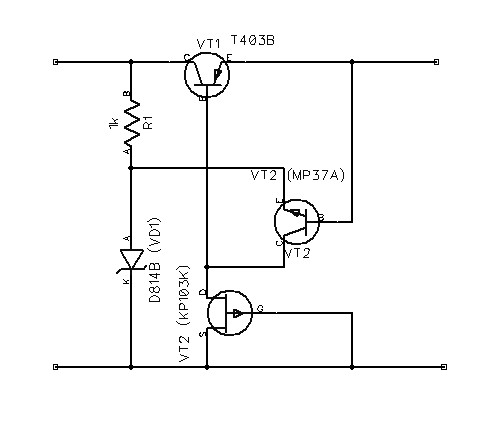
The schematic diagram originates from a voltage regulator circuit utilizing a Field Effect Transistor (FET) power supply. This circuit features a feedback mechanism involving the FET VT3, which functions as a dynamic load for transistor VT2. This configuration enhances...
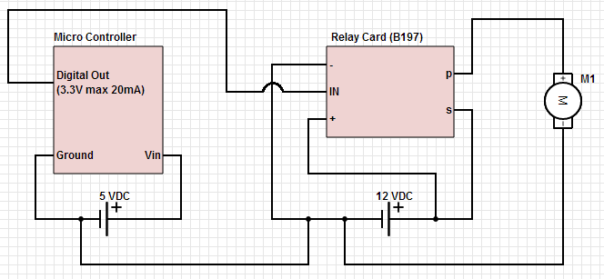
The objective is to control a 12 VDC device (on/off) from a microcontroller using a relay card. The relay requires a 12 VDC operating power supply. To achieve the control of a 12 VDC device using a microcontroller and a...
All miniature electronic devices operate off batteries. Some of them require higher than the standard battery voltages to function efficiently. Miniature electronic devices, which include a wide range of applications from portable gadgets to remote sensors, typically rely on battery...
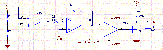
This circuit enables a smaller control voltage to inversely and linearly control a larger output voltage (Vo). Additionally, the supply voltage (Vsp) for the operational amplifiers can be lower than the output voltage, allowing the circuit to theoretically control...
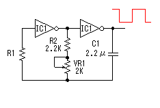
This circuit is a square wave oscillator that utilizes CMOS-type logic inverters. The term "logic inverter" is used to prevent confusion with a DC/AC inverter. The oscillator's output is connected to a drive circuit via the logic inverters. The...
The LM2889 is designed to interface audio and video signals to the antenna terminals of a television receiver. It consists of a sound subcarrier oscillator, an FM modulator, a video clamp, and RF oscillators and modulators for two low-VHF...