
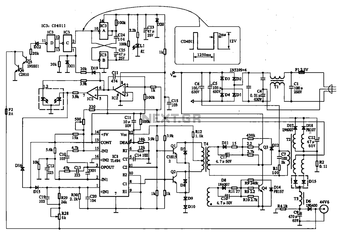
Make circuit of the inverter and operating principle by oneself
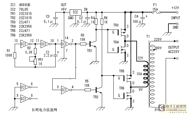
The inverter circuit design employs a MOSFET to achieve efficient conversion of DC to AC power, suitable for various applications, particularly in electronic fans. The MOSFET operates by controlling the output current through voltage modulation at its gate terminal, which significantly enhances the input impedance and allows for minimal power loss. The integration of the CD4069 as a signal generator is crucial, as it produces a stable rectangular wave that drives the MOSFET. The compensating resistor R1 plays a vital role in maintaining frequency stability, ensuring that the inverter operates effectively despite variations in the mains supply.
The capacitive component C1 is essential for managing the timing of the charge and discharge cycles, directly influencing the oscillation frequency. The calculated maximum and minimum frequencies provide insight into the operational bandwidth of the inverter, indicating its capability to handle varying load conditions efficiently. The phase shifter component is strategically implemented to mitigate potential interference, ensuring that the inverter can coexist with other electronic devices without degradation of performance.
The use of TR1 and TR2 for voltage amplification allows the inverter to output a higher voltage, necessary for driving loads that require more power. The design emphasizes the importance of selecting appropriate components to ensure reliability and efficiency in operation. Overall, this inverter design represents a practical solution for applications requiring reliable power conversion, leveraging the advantages of MOSFET technology and careful circuit design principles to achieve optimal performance.We introduce an inverter today mainly by the MOS field effect tube, the ordinary power transformer forms. Its output power depends on the power of MOS field effect tube and power transformer, avoid the convoluted voltage transformer to wind, suit electronic fan`s spare time to adopt while making.
Now introduce operating principle and fabrication process of this voltage transformer. Adopt CD4069 and form the signal generator of rectangular wave here. R1 is the compensating resistance in the circuit, it is unstable in frequency to use for improving the shock caused by change of the mains voltage. The shock of the circuit charged and discharged to finish through the electric capacity C1. Its oscillating frequency is f =1/2. 2RC. The maximum frequency of the diagramatic circuit is: fmax=1/2. 2x103x2. 2G—10- 6 =62. 6Hz, the minimum frequency is fmin =1/2. 2G—4. 3x103x2. 2G—10- 6 =48. 0Hz. Because of the error of the component, actual value will have some the difference. Other surplus sending to the phase shifter, earth and avoid influencing other circuit in the input end.
Because the maximum crest of signal voltage of vibration that the rectangular wave signal generator outputs is 0~5V, for drive the intersection of power and switching circuit fully, here use TR1, TR2 the intersection of oscillating beacon and voltage amplification to 0~12V. As shown in Fig. 3. The field effect tube is a core of this device, before this part of operating principles in the introduction, explain the operating principle of the MOS field effect tube briefly first.
The MOS field effect tube is known as MOS FET too, namely Metal Oxide Semiconductor Field Effect Transistor metal oxide semiconductor field effect tube Abbreviation. It generally has two kinds of depletion modes and enhancement types. What this text used is an enhancement mode MOSFET, its internal structure is shown in Fig. 4. It can be divided into N-P-N type and P-N-P type. The N-P-N type is usually called N channel type, the P-N-P type usually calls P channel type. Can find out, connect on the N-type semiconductor as to its source and drain of the field effect tube of N channel type from pursuing, connect to its source and drain of the field effect tube in the p-channel on the P-type semiconductor too.
We know the general triode is the electric current exported by the current control importing. But to the field effect tube, its output current is from the voltage or the field voltage that is input Control, can be thought the minima of input current or not had input current, this makes this device have very high input impedance, this is our reason known as field effect tube too at the same time. In order to explain the operating principle of the MOS field effect tube, we know first that only working phase including diode of one P-N knot.
As shown in Fig. 5, we know and add in the diode to direct voltage P head joint positive pole, N head joint negative pole When, the diode is turned on, its PN junction has passing of current. This is because when the end of P-type semiconductor is the positive voltage, the N-type semiconductor inner negative electron is attracted and poured into the end of P-type semiconductor with positive voltage, and P-type semiconductor carry inner positive electron take exercises towards the intersection of N-type semiconductor and end, thus take shape, lead alive.
The same, look on as the diode and add the backward voltage P head joint negative pole, at the time of N head joint positive pole, it is the negative voltage on the end of P-type semiconductor at this moment, the positive electron is assembled on the end of P-type semiconductor, the negative electron assembles on the end of N-type semiconductor, the electron does not move, its PN junction does not have electric current that flow through, the diode ends. As to the field effect tube Fig. 6, Without voltage in the grid, it is knowing that 🔗 External reference
Related Circuits
Full sine wave UPS information in English, along with detailed C language source code. English proficiency may be a concern, so caution is advised. A full sine wave Uninterruptible Power Supply (UPS) is designed to provide a stable and continuous...
LED sequencer that follows the rhythm of music or speech, powered by a 9V battery, is a portable unit. The basic circuit illuminates up to ten LEDs in sequence, following the beat. The LED sequencer circuit operates by detecting audio...
The delay time ranges from 0.5 to 3.5 seconds, which can be adjusted using the potentiometer RP to modify the delay duration. The circuit utilizes a timing mechanism that allows for the adjustment of delay intervals between 0.5 seconds and...
The TN-1 Intelligent Negative Pulse Charging Circuit is a sophisticated device designed for efficient battery charging. It operates as a half-bridge charger, which is a common configuration in such circuits. The negative pulse charging mechanism is facilitated by a...
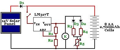
The circuit is designed to power a CCTV camera, provide lighting inside a nestbox, and charge batteries using a photovoltaic (PV) solar panel. It includes a circuit diagram for a solar-powered wireless CCTV camera with battery backup. D1 is...
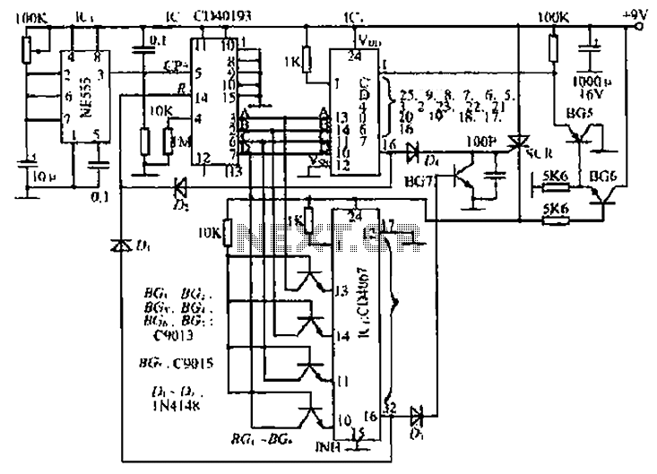
The circuit consists of an oscillator, a counter, and an Iseki circuit divided into three parts. The oscillator is based on the NE555 timer and several external RC components, generating a pulse signal for the counter. The instantaneous power...