
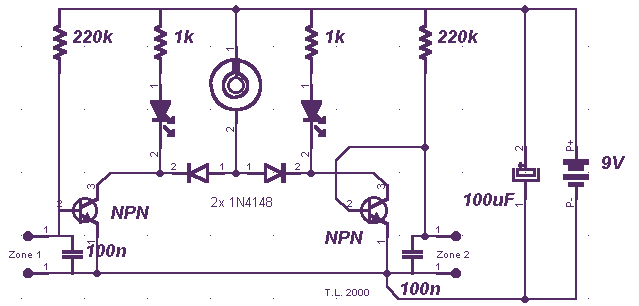
Miniature Loop Alarm
The circuit in question utilizes a simple transistor switch configuration, which is well-suited for applications requiring low power consumption and compact design. The implementation begins with selecting an appropriate transistor, typically a bipolar junction transistor (BJT) or a field-effect transistor (FET), based on the required switching characteristics and load specifications.
In a basic transistor switch circuit, the transistor operates in either the cutoff region (off state) or the saturation region (on state). The input signal is applied to the base (for BJTs) or the gate (for FETs) of the transistor, controlling its conductive state. A resistor is often placed in series with the base or gate to limit the input current, ensuring the transistor operates within safe parameters.
The load is connected to the collector (for BJTs) or the drain (for FETs) of the transistor, and a power supply is connected to the emitter (for BJTs) or the source (for FETs). When the input signal is high, the transistor turns on, allowing current to flow through the load, which can be an LED, motor, or any other device requiring activation. Conversely, when the input signal is low, the transistor turns off, cutting off the current to the load.
The advantages of this configuration include simplicity in construction and a minimal number of components, which contributes to the overall reliability of the circuit. The low power consumption is achieved by ensuring that the transistor remains in cutoff when not actively switching, thus drawing negligible current from the power supply.
For applications where size is a critical factor, surface-mount devices (SMD) can be employed to further reduce the footprint of the circuit. Additionally, careful layout design can minimize parasitic capacitance and inductance, enhancing the performance of the switching action.
In summary, the circuit leverages the switching capabilities of transistors to achieve a reliable and efficient solution for various electronic applications, emphasizing simplicity, low power consumption, and compactness.Simple construction, reliable operation, very small power consumption, and, most of all, small size. I started with CMOS logic gates, but was soon forced to abandon the concept after a few unsuccessful (and far too complicated) attempts. Then I suddenly realized that a simple transistor switch might do the job and I was right. 🔗 External reference
Related Circuits

When the protective circuit is interrupted (opened), the alarm sounds. To set the circuit, adjust R2 (with the protective circuit open) for 1 V across R1. The described circuit functions as a protective alarm system that activates when the integrity...
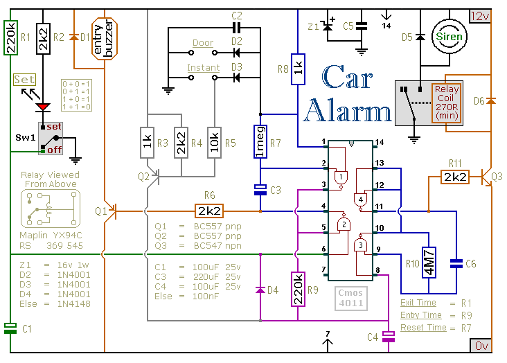
The alarm is set by opening Sw1. It can be any small 1-amp single-pole change-over switch - but for added security, you could use a key-switch. Once Sw1 is opened, you have about 10 to 15 seconds to get...

The light-sensitive CDS cell R8 is configured in a bridge circuit with IC1 functioning as a comparator. When light strikes the CDS cell R8, the output of IC1 goes high, triggering SCR1. This action illuminates LED1 and activates opto...

The circuit timer with a musical alarm utilizes a well-known CMOS oscillator/divider integrated circuit (IC1). Although this circuit operates at 9V, its standby current drain is minimal. The time delay of the timer circuit can be adjusted by modifying...
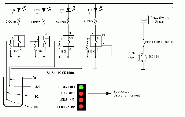
This circuit indicates the water level in an overhead tank and activates an alarm when the tank is full. It utilizes the commonly available CD4066 bilateral switch CMOS IC to display the water level through LEDs. When the tank...
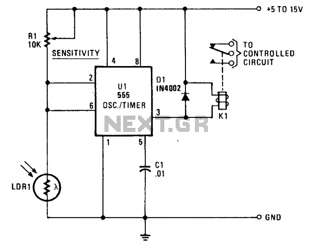
LDR1, a cadmium sulfide (CDS) photoresistive cell, is utilized as the lower leg of a voltage divider between Vcc and ground. The timer terminals 2 and 6 are connected to the junction of the photocell and the sensitivity control...