
Mobile Phone Charger with CA3130
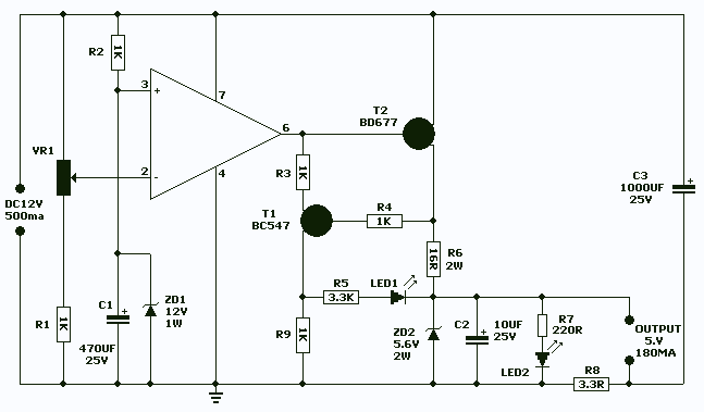
The circuit operates as a protective interface between a mobile phone and a standard charger, ensuring safe charging while mitigating risks associated with voltage fluctuations. The main components include the CA3130 operational amplifier, which functions as a voltage comparator to monitor input conditions. The variable voltage from the potentiometer VR1 allows for fine-tuning of the system response based on the specific battery characteristics.
The delay mechanism provided by capacitor C1 ensures that the circuit does not immediately resume operation after a power outage, which can prevent potential damage from transient voltages. The zener diode ZD1 serves a critical role in voltage regulation, acting to clamp excessive voltages that could harm the connected devices.
The output from the CA3130 drives the BD677 transistor, which acts as a switch for the charging current. The current-limiting resistor R6 is crucial in maintaining the charging current at a safe level of approximately 180mA, which is optimal for the battery's longevity. Zener diode ZD2 further stabilizes the output voltage at 5.6V, ensuring that the battery charges effectively without exceeding its voltage rating.
LED indicators provide visual feedback on the circuit's operational status. LED1 signals an over-current condition or short-circuit, while LED2 indicates that the battery is currently being charged. The design allows for adjustments to the charging current through the selection of resistor R7, providing flexibility depending on the specific battery requirements.
Overall, the circuit is designed to enhance the safety and efficiency of mobile phone charging while extending battery life through controlled charging practices. Proper assembly on a PCB and housing in a protective case is recommended to ensure durability and reliability during operation.The circuit described here provides around 180mA current at 5.6V and protects the mobile phone from unexpected voltage fluctuations that develop on the mains line. So the charger can be left ?on? over night to replenish the battery charge. The circuit protects the mobile phone as well as the charger by immediately disconnecting the output when it senses a voltage surge or a short circuit in the battery pack or connector.
It can be called a ?middle man? between the existing charger and the mobile phone. It has features like voltage and current regulation, over-current protection, and high- and low-voltage cut-off. An added speciality of the circuit is that it incorporates a short delay of ten seconds to switch on when mains resumes following a power failure.
Most mobile chargers do not have current/voltage reguLation or short-circuit protection. These chargers provide raw 6-12V DC for charging the battery pack. Most of the mobile phone battery packs have a rating of 3.6V, 650 mAh. For increasing the life of the battery, slow charging at low current is advisable. Six to ten hours of charging at 150-200mA current is a suitable option. This will prevent heating up of the battery and extend its life. This protects the mobile phone from instant voltage spikes. The circuit is designed for use in conjunction with a 12V, 500mA adaptor (battery eliminator). Op-amp IC CA3130 is used as a voltage comparator. It is a BiMOS operational amplifier with MOSFET input and CMOS output. Inbuilt gate-protected p-channel MOSFETs are used in the input to provide very high input impedance. The output voltage can swing to either positive or negative (here, ground) side. The inverting input (pin 2) of IC1 is provided with a variable voltage obtained through the wiper of potmeter VR1. The non-inverting input (pin 3) of IC1 is connected to 12V stabilised DC voltage developed across zener ZD1.
This makes the output of IC1 high. After a power resumption, capacitor C1 provides delay of a few seconds to charge to a potential higher than of inverting pin 2 of CA3130, thus the output of IC1 goes high only after the delay. In the case of a heavy power line surge, zener diode ZD1 (12V, 1W) will breakdown and short pin 3 of IC1 to ground and the output of IC1 drops to ground level.
The output of IC1 is fed to the base of npn Darlingtontransistor BD677 (T2) for charging the battery. Transistor T2 conducts only when the output of IC1 is high. During conduction the emitter voltage of T2 is around 10V, whichpasses through R6 to restrict the charging current to around 180 mA.
Zener diode ZD2 regulates the charging voltage to around 5.6V. When a short-circuit occurs at the battery terminal, resistor R8 senses the over-current, allowing transistor T1 to conduct and light up LED1. Glowing of LED2 indicates the charging mode, while LED1 indicates shortcircuit or over-current status.
The value of resistor R8 is important to get the desired current level to operate the cut-off. With the given value of R8 (3.3 ohms), it is 350 mA. Charging current can also be changed by increasing or decreasing the value of R7 using the ?I=V/R? rule. Construct the circuit on a common PCB and house in a small plastic case. Connect the circuit between the output lines of the charger and the input pins of the mobile phone with correct polarity. 🔗 External reference
Related Circuits
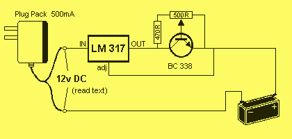
This circuit will charge a 12v battery (10 NiMH cells) @ approx 220mA. It is a very simple circuit but requires correct setting up. The circuit is designed around a 12vDC, 500mA plug pack. This type of plug pack...
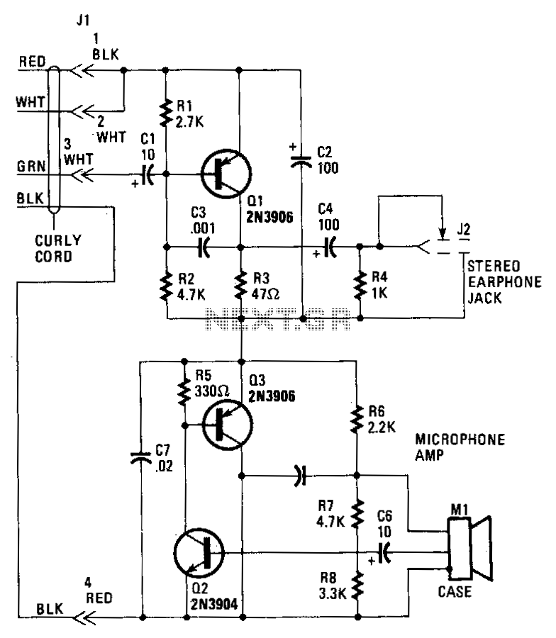
Transistor Q1 in the headset amplifier circuit amplifies the 30 mV signal intended for the earphones to 0.5 V, which is sufficient to drive stereo earphones. Capacitor C1 blocks any DC current from shorting back into the telephone base....
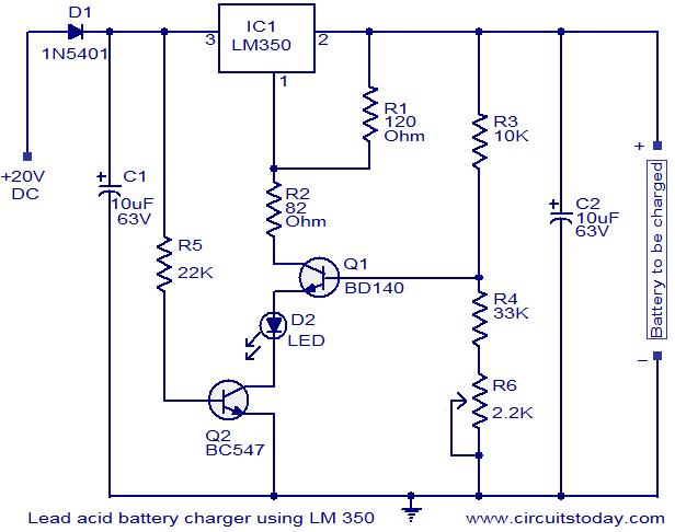
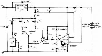
This circuit utilizes the IC LM350 for charging 12V lead-acid batteries, providing a constant voltage source with a negative temperature coefficient. The transistor Q1 (BD140) functions as a temperature sensor, while transistor Q2 prevents the battery from discharging through...
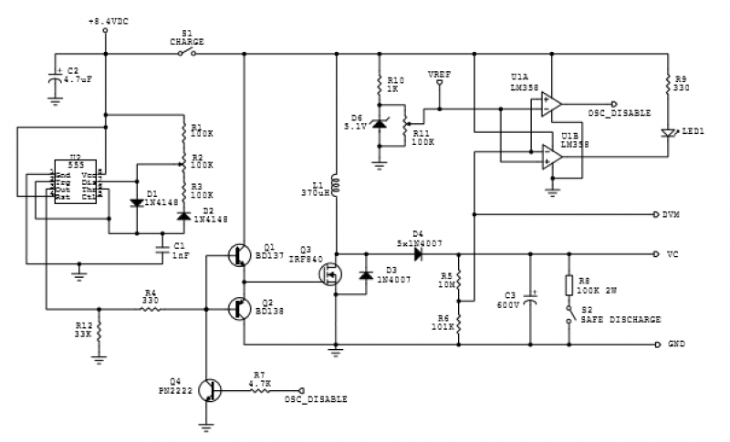
The circuit described utilizes an IRF840 MOSFET, which has a maximum drain-source voltage (DSV) rating of 500V. The avalanche voltage is calculated to be approximately 365V, indicating that inductive kickback voltage can reach up to about 600V in the...

Any phone can be utilized for this project, so there is no need to worry about obtaining the same model as mentioned. If an antique Bakelite phone is chosen, basic restoration steps include cleaning it with a rag dampened...
This circuit provides an initial voltage of 2.5 V per cell at 25°C to quickly charge the battery. As the battery charges, the charging current decreases, and when it drops to 180 mA, the charging circuit reduces the output...